This thread has been locked.

If you have a related question, please click the "Ask a related question" button in the top right corner. The newly created question will be automatically linked to this question.

DRV8353: Enable toggling caused output voltage shifting

Part Number: DRV8353

Dear Teams,

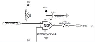
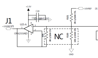
My customer is using DRV8353. When they toggle the enable signal, such as change from enable to disable or reverse, they found the output voltage sometimes is 1.5V, sometimes will be 1.51V. They set the ref voltage to 3V without any changes. Could you help give some suggestions why output voltage sometimes will go to 1.51V? The probability of 1.51V event occur is around 10%. You can find the schematic diagram here:

Thanks!

Dylan

  • Hello Dylan,

    Thank you for the info and for posting on the MD forum. I am glad to help you work through this issue, just a couple of questions on my end:

    Is there a specific reason why the customer is using a voltage follower circuit here, such as are there several device pins connected to this 3.0V reference buffer circuit? I cant tell from these images exactly how the enable pin is connected, so if you had more info on this that might be helpful. I assume that this should be the only pin connected to this 3V reference, is the positive pin on the op amp connected to a GPIO pin from an MCU?

    Best,

    Isaac

  • Hi Lara,

    Thanks a lot for your prompt reply! The voltage follower is used to give power supply for DRV8353's Vref. They used jumper wire to connect the enable to 3.3V or GND to change the status of enable/disable. Do you have any suggestions or see any similar case before that output voltage might not be exactly 1.5V if we toggle enable pin?

    Thanks!

    Dylan

  • Hello Dylan,

    Thank you for clarifying the information about the voltage follower, I see the connection to VREF. I have not seen this case before and was not able to find any other threads with a similar case. Just a couple of questions/ suggestions to try:

    Does the device stay at 1.5V the entire time or does it last for a determine amount of time? There is an internal pulldown on the ENABLE pin, perhaps this could have something to do with it, if they are connecting it directly via a wire from 3.3V have they tried using a pullup resistor in the path to pull it up to 3.3V?If other pins are sharing this 3.3V rail have they tried separating the ENABLE pin to its own 3.3V rail to see if the problem is still being observed? 

    Has the customer seen this on multiple devices or has it been on just one?

    Best,

    Isaac

  • Hi Lara,

    Once they toggle the enable, the output will keep at 1.5V or 1.501V all time. The rest of questions I am checking with my customers.

    Thanks!

    Dylan

  • Hi Lara,

    Once they toggle the enable, the output will keep at 1.5V or 1.501V all time. They control the enable signal and external fault signal simultaneously. They used REF5030AIDGKR to give 3.0 Vref. They used zero-drift follower to output to the DSP's Vref and driver chip's Vref.

    Thanks!

    Dylan

  • Hi Isaac,

    Sorry for I forget to update enable circuit in previous reply. Please check it here

  • Hey Dylan,

    What do you mean by they control the enable signal and the external fault signal simultaneously? The nFAULT signal coming out of the DRV8353  just needs to be pulled up and this will automatically pull down low in the case of a fault condition, so I am just trying to figure out what you mean. Did you mean that the nFAULT and ENABLE share the same VCC supply? So, VREF is being shared between the DRV and a processor, but is this same VREF being used to pullup nFault and ENABLE? 

    Having the full schematic here to review here would be helpful. My concern is that if this same VREF from the REF5030AIDGKR is being shared amongst various inputs and devices it is possible that it is getting loaded and that is why you see the voltage drop to ~1.5V at certain conditions and perhaps this is why they have only been able to see this happen 10% of the time.

    Also keep in mind that ENABLE does not need to be pulled up the way it is here, normally you want this pin to be connected to the MCU in order to be able to enable and disable the device, so the MCU is providing the 3.3V signal needed. I made the recommendation to pull it up earlier since it sounded like this was not connected to an MCU at the moment. If this is connected to an MCU (as it looks like here) is it possible the MCU settings on the GPIO it is connected to could be altering the behavior?

    Just to recap if you could provide full schematics it might be easier to help troubleshoot. If you do not feel comfortable sharing the entire schematics on here feel free to send me a friendship request.

    Best,

    Isaac

  • Hello Dylan,

    Do you need any further help on this thread?

    Thanks,

    Matt

  • Hi Hein,

    May not now.

    Thanks!

    Dylan

  • Thanks, I'll close this thread for now. If you have further questions, please click the "Ask a related question" button!

    Thanks,

    Matt