This thread has been locked.

If you have a related question, please click the "Ask a related question" button in the top right corner. The newly created question will be automatically linked to this question.

DRV8350F: DRV8350F SHx Overshoot / Ringing

Part Number: DRV8350F
Other Parts Discussed in Thread: DRV8320, , DRV8350, DRV8353, DRV8353F, ALLIGATOR

Hi,

I already had a board a few month ago with the same problem, where I used a DRV8320 (e2e.ti.com/.../drv8320r-drv8320r-how-much-rining-is-good-enough) and now I use the DRV8350F  for 80V compatibility (more safety margin for the 48VDC Input).

I tought the problem came from a bad layout, too much parasitic inductance, but now the design is way better and the ringing is worse (probably from the MOSFETs, changed from 60V MOSFETs to 80V MOSFETs). It seems like the gate driver overshoot before the Miller Plateau and couples into the output and leads to the overshoot of SHx, but I'm already on the minimum IDRIVE setting of 50mA/100mA, so it seems this gate driver does not work with the MOSFETs I have chosen: BSC040N08NS5ATMA1

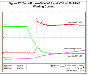
I get a significant overshoot at already 12A phase current, only 10V is allowed and I get around 8V. When I go higher, it begins to overshoot the 10V mark. I need to achieve 50A, impossible at the moment.

I'm thinking about using some series resistors for the gate, that could probably solve the problem, but it is not recommended in the datasheet. For example this guy here in this thread uses gate resistors and can easly achieve 100A: https://e2e.ti.com/support/motor-drivers-group/motor-drivers/f/motor-drivers-forum/915569/drv8350-own-hardware-with-drv8350

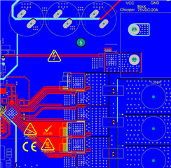
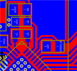
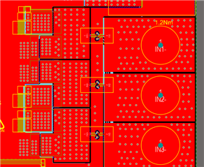
Here is an overview of the design, I used the “Best Practices for Board Layout of Motor Drivers” PDF and the datasheet for the design to achieve low inductance paths and it seems also all the cross coupling is gone from other MOSFETs, but this ringing is I can not get rid off:

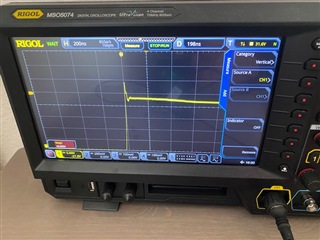
Here is some Overshoot/Ringing from SHA (measured with a GND spring):

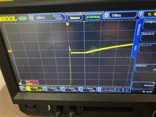
And here some Overshoot/Ringing on the GHA (measured with a GND spring):

So, what can I do about this? Are gate series resistors a solution? Shold I change the FETs? Are Snubbers necessary?

Kind Regards,

Sebastian 

  • Hello Sebastian,

    Thanks for the questions. Just to mention it might not be necessary to use the DRV8350F instead of the DRV8350 unless if you are planning on using for functional safety. Here is a thread summary you can read, this goes over the differences in DRV8353 and DRV8353F which are essentially the same device but with current sense amplifiers: https://e2e.ti.com/support/motor-drivers-group/motor-drivers/f/motor-drivers-forum/1004843/drv8353f-is-drv8353f-pin-compatible-with-drv8353s

    That being said moving to 80V versus 60V is a good change which will give you additional margin when operating at 48V.

    In the thread that you linked: https://e2e.ti.com/support/motor-drivers-group/motor-drivers/f/motor-drivers-forum/915569/drv8350-own-hardware-with-drv8350 it is important to note that this user indicated that the resistors he had in the gate drive path were actually populated with 0 ohm resistors. The thing I would highlight about this thread is that there seems to not been much inherently wrong with their adaptation of the device but mainly the way that they were making their measurements, the ringing seemed to be associated with their ground pin on their probe and used a ground spring to make the measurement and the ringing was not there anymore. This can happen because the alligator clips on scope probes generally add inductance. So using a ground spring with your system will help you display the ringing more accurately, if you have not already tried this I would definitely give it a shot in order to accurately asses the ringing in your system.

    The next set suggestion would be to review our System Design Considerations for High-Power Motor Driver Applications App note, this goes over some ringing mitigation techniques. Like mentioned RC Snubbers are a good way to reduce the settling time of a ringing node as well bulk capacitance.

    Let me know if this helps!

    Best,

    Isaac

  • Hi Isaac,

    Thanks for the answere. I implement a STO function with puls blocking, so the DRV8350F is the right choice.

    The user in this thread seems to use some snubbers (3.3Ohm, 33nF), so that might be the real difference. I will test snubbers soon and also add additional bulk directly next the FETs. Further, it seems the gate current settings are all in all very high for the DRV8350, for my FETs I would think 25mA/50mA would already fit. Maybe I can change to higher Qgd MOSFETs to reduce the overshoot?

    The measurements should be fine, already done with a spring probe next to the FETs, so the overshoot seems critical, since this is not the maximum current I would like to drive. 

    Kind Regards,

    Sebastian

  • Hey Sebastian,

    Awesome, just wanted to make sure that you were using the best device suited for your needs.

    We have an FAQ that you can review on how to choose values for you RC Snubber circuit. I will link it here so that you can refer to this material when designing a snubber that fits your system best. If the IDRIVE current seems high you can always use a gate resistor to see if that helps, normally we recommend this if you are trying to fine tune your system or if the IDRIVE settings are too high, but it might be best to test the snubber first as well as the added bulk capacitance to see if they help significantly reduce the overshoot you are seeing on your system. I am not sure if getting a MOSFET with a higher Qgd will help you reduce overshoot. I can look into this an get back to you on this item.

    Sorry I just realized you included that you made the measurements with a GND spring, I must have missed that in my first pass.

    Best,

    Isaac

  • I could now improve my overshoot by using a snubber network, but I would prefer a solution without. I tried to improve the ringing by adding a 100uF bulk cap directly at the supply of the high side MOSFETs, but that did not improve anything, so I think the bulk is not the problem here. What I will do in the next iteration is to increase the trace width for all the signals to the MOSFETs, this should nearly half the inductance as I have it now and hopefully reduce also the ringing. But before I order new hardware, I want to fully understand what is really going on.

    I had now also a look at different reference designs from TI and I see, there is significant ringing, but it seems not to be a problem at all.

    If we have a look at https://www.tij.co.jp/lit/ug/tidueq9a/tidueq9a.pdf?ts=1632754718461&ref_url=https%253A%252F%252Fwww.google.com%252F, (Figure 27). you can see, that there is some ringing ongoing, also with the designed snubber:

    So here the input voltage ist +54VDC and the peak goes here up to around +68VDC, way over the threshold of +10VDC @200ns in the datasheet. How is this 200ns, +-10V threshold defined? When this is energy based, can I safely go for 20ns into +- (V^2 * t) +-31.62V? 

    Further, I found this reference design here:

    https://www.ti.com/lit/ug/tidue60/tidue60.pdf?ts=1632754162076&ref_url=https%253A%252F%252Fwww.google.com%252F

    There seems to be a soft and hard swichting ongoing, but it is not stated, what this means? Has it to do with the IDRIVE setting or using the snubber network?

    Kind Regards,

    Sebastian

  • Hello Sebastian,

    Thanks for the update, I am sorry hear  there was not much improvement when adding the snubber or the extra bulk capacitance. I believe the main issue you should reconsider is definitely your layout. Not only increasing the trace widths but decreasing some trace lengths can help you drastically improve your ringing. 

    Here is this app note you can read for best practices for board layout: https://www.ti.com/lit/an/slva959a/slva959a.pdf 

    It is very difficult to have a system with no ringing, this is typically something you will occur due to all the patristic inductance found in the system, decreasing this parasitic inductance significantly decreases ringing. In the image you referenced there does seem to be ringing above the +10 mark that is advised, but perhaps because it is less than 200ns it does not cause an issue? I would have to check internally how this specification is defined. I am not sure where you obtained the +-(V^2*t) formula from but I will check if there is a way to calculate the limit of the ringing if it the duration extremely short.

    I am not too familiar with this subject but I found this TI Training video on soft switching in order to help you understand what the soft switching concept is: https://training.ti.com/soft-switching

    Hard switching seems to be the type of switching that you have been doing to the all along and soft switch is where the goal is to get the voltage to zero before the switch is turned on.

    Best,

    Isaac