


Hi Team,
Section 8.3.1.3 of the datasheet states that if VM is less than 12V, VVCP = 2 x VVM-1.5V. Example, If VM is 10V then VVCP = 2 x 10 - 1.5V = 18.5V. Is this correct?
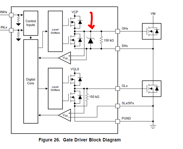
However, the Figure 26 of the DRV8323 datasheet shows the VCP pin is connected to the Drain pin of the internal high-side MOSFET. Therefore the output to the GHx pin will exceed the VGS of the external MOSFET. Is the VCP pin in Figure 26 supposed to be VGSH? If not, how is the output at GHx pin regulated to within the limit of VGS of the external MOSFET?
Regards,
Danilo


 ,
,