This thread has been locked.

If you have a related question, please click the "Ask a related question" button in the top right corner. The newly created question will be automatically linked to this question.

DRV8305-Q1: with a brushed motor

Genius 4680 points
Part Number: DRV8305-Q1

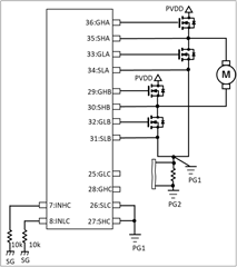
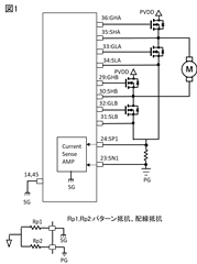
Can the DRV8305-Q1 be used with a brushed motor (single phase)?

If Yes, the remaining 1 phase terminals (GH_C, SH_C, GL_C, SL_C)

Is it okay to process empty terminals with OPEN?

Regards

Kura

  • Hi Kura-san,

    Yes you can use a single phase brushed DC motor. Connect other end to PVDD or GND for unidirectional control with HS or LS driver. 

    Please short SHC and SLC to GND, and float GHC and GLC. This will ensure VDS_OCP is never triggered since VDS = 0V and VGS = 0V, as long as you don't turn on phase C's INHC/INLC signals. 

    Thanks,
    Aaron


  • Aaron-san

    Thank you for your support.

    We got additional questions.

    Question1:

    They are thinking of pulling down INHC and INLC with external resistors, is that a problem?

    We would appreciate it if you could give us your opinion for reference.

    Question2:

    It is said that SLC and SHC are short-circuited to GND. Can you give us an idea of which GND to connect to?

    Customer Thoughts: Connect to PG1

    Reason) When connected to PG2, due to the potential difference of the current detection resistor 

    VDS_OCP may malfunction, so connect to PG1.

    Regards,

    Kura

  • Hi Kura-san,

    Q1: Yes you can pull down with external pulldown resistors. 
    Q2: It should be connected to PGND. Can you explain what PG1 and PG2 is or show a diagram?

    Thanks,
    Aaron

  • Aaron-san

    Thank you for your support.

    I attached diagram that shows PG1 and PG2 .

    Please check attached.

    regards,

    Kura

  • Hi Kura-san, 

    This diagram looks good, you should connect to PG1 because shunt resistor can trigger voltage potential that couples into the SLx trace, which could trigger overcurrent if monitoring with respect to PG2. Connect SLC = SHC = PG1. INLC and INHC look good too. Ensure SG, PG1, and PG2 have minimal voltage potential difference between split grounds. 

    Thanks,
    Aaron

  • Aaron-san

    Thank you for your support.

    We got additional questions from customer.

    Please advise us following.


    1.About current detection (SP1, SN1) in the pre-driver
    The description is that the common mode input range is -0.15 to 0.15V, but if the common mode input range is exceeded (for example, 0.4V common mode input).What will happen to the output voltage (SO1)?


    2.About the wiring resistance of GND when using the current detection in the pre-driver

    If, in the system configuration shown in Figure 1, they use current detection in the pre-driver, does the resistance of Rp2 at 40A current detection have to be within 3.75mΩ (0.15V / 40A)?

    3.Pre-driver-SPI register setting PWM_MODE
    For the system configuration shown in Figure 1 (motor driven with a single-phase brush), which mode should they use?
    Also, could you briefly tell us about this mode?

    Regards,

    Kura

  • Hi Kura-san, 

    1) I think these ranges exists due to the CSA gain settings, with the min setting = 10V/V. If common input exceeds +/-0.15V, then if VREF = 3.3V and G = 10, then Vo = +/-1.5V and this would be at the limits of the linear range of the SOx output. I think you may be able to marginally exceed +/- 0.15V if VREF is 5.0V rather than 3.3V. I need to confirm why this spec is written this way.

    2) For current detection in the pre-driver, are you referring to VDS_OCP or SNS_OCP? Is Rp1 or Rp2 the shunt resistor?

    For VDS_OCP, the equation for overcurrent to trigger is I_DS * Rds_on > VDS_OCP
    For SNS_OCP, the equation for overcurrent to trigger is 2V > SL_x - GND, where SL_x - GND = I_shunt * R_shunt. 

    This also assumes that the layout is good enough so there isnt a ground potential difference to cause noise at SL_x or GND, and ensuring that if there is ground potential difference, the durations of the noise are shorter than OCP deglitch times. 

    3) For a Brushed_DC motor, you should have control over each half bridge. This means you should use 6x PWM mode or 3x PWM mode (setting 00b, 01b, or 11b). 

    Thanks,
    Aaron

  • Aaron-san

    Thank you for your reply.

    1)VREF is used at 5V. Please provide the reason for the data sheet description and give us the specifications when VREF = 5V.

    2)It is about SP1 and SN1. Rp1 and Rp2 are wiring resistors for harnesses, etc.

    3)They understand setting.

    Regards,

    Kura

  • Hi Kura-San,

    Allow me to provide a response tomorrow.

    thanks, Aaron

  • Aaron-san

    If you have any update for this,please let us know it

  • Hi Kura-san,

    Sorry for the delay in reply. 

    1) VIN_COM is the offset from SPx/SNx to GND seen by both inputs, and which should not be visible in the SOx output. The common mode input range is how much common mode can be applied to SPx/SNx while operating within spec. For example, if you tie SNx/SPx together, the output should be at VREF/k, and then if you vary the offset of SNx/SPx to GND, you shouldn’t see SOx move as long as you stay within the common mode spec. VIN_COM is valid for all gain settings, unrelated to the output voltage or VREF division setting. However, the actual circuit limitation is due to a body diode path between SPx/SNx to SOx, so it can be exceeded in certain situations. 

    2) For the wiring resistors for harnesses, I would ensure that the resistance difference between PG and SG is negligable in that there is not there is not a voltage potential difference that causes incorrect current measurements. 

    For instance, if Rp1 = Rp2 = 1 ohm, then there will be Rp_eq = 0.5ohm resistance between signal GND and SG/PG. If signal GND goes to MCU, and SG/PG sees 50mV (i.e. V_Rp = I_motor * Rp_eq), then then the SOx calculation will be 50mV inaccurate to calculate current feedback. You would also need to ensure added inductance is not introduced from the wiring harness, or else this may cause voltage spiking when motor current is switching. 

    Thanks,
    Aaron

  • Aaron-san

    Thank you for your reply.

    The reason why there is a limitation of VIN_COM is that there is a body diode from SPx / SNx to SOx.
    Could you please show us the internal circuit diagram with the description of the body diode of the SPx / SN terminal?

  • Hi Kura-san,

    The information about the body diode and diagram is shown in the snippet below.


    Thanks,
    Aaron