This thread has been locked.

If you have a related question, please click the "Ask a related question" button in the top right corner. The newly created question will be automatically linked to this question.

DRV8304: Question about AutoCal for automatic offset cancellation

Part Number: DRV8304

Hi team,

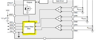
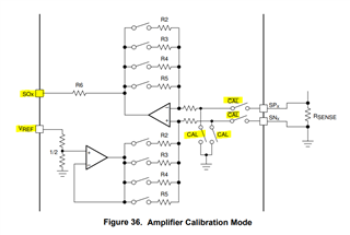
I want to know how AUTOCAL works? After AUtoCAL started, what kind of operation did the op amp perform? (In addition to connecting the input to ground), how do we perform the calibration? (Adjusted the internal resistance?), do we have any information on this function

Thanks

Jenson

  • Hi Jenson, 

    Will look into this and follow up soon with a response 

    Thanks and Best Regards,

    Andrew

  • Hi Jenson,


    Please see the below response:

    • in terms of the 'calibration' feature, I will send you an email with our systems team to see if we can arrive at an answer for this quickly  
      • (will be out of office in a few days, so I just want to make sure you are able to get an answer from my other teammates if I'm not present to respond) 
         
    • Fundamental operation: 
      • Datasheet describes that the calibration sequence works by:
        • disconnecting the amplifier inputs from the SPx/SNx pins and shorting them internally to GND
          • The purpose of this is to set a true zero-voltage-differential in the inputs of the amplifier
          • In an ideal situation, we would expect the output to reflect that there is no input offset either
          • However, because of non-ideal process variation and temperature shift, this output is also non-ideal
      • At this time, there is probably some measurement of this non-ideal amplifier output 'error' value
        • My best guess is that this baseline 'error' measurement is stored internally in the device's memory,
          so that it can be subtracted from every CSA measurement during regular operation (while the device is not performing calibration)
        • The systems team should be able to help clarify this, whether it's some memory registers to store the offset, or some resistance changes like you suggested


    Datasheet image of device block diagram, focusing on CSA gain section


    CSA circuit diagram

    • Figure demonstrates the calibration 'switches' that are toggled, and also how the Vref input voltage and gain setting resistors affect output SOx


    Thanks and Best Regards,

    Andrew

  • Hi Jenson,

    followed up with the systems on this offline - looks like there isn't much detailed information on the internal workings on the device design/history. 

    Like mentioned in my earlier response, there's probably either:

    1. some mechanism to store the calibration 'error' offset so that it can be subtracted from other measurements later on 
    2. or it could be a 'trim' type optimization where some internal trim circuit will try out different CSA configuration settings to at least minimize this error during the calibration sequence. and then this best-fit trim setting will stay in place until a new autocal sequence is run to override the old settings 

    Best Regards,
    Andrew