This thread has been locked.

If you have a related question, please click the "Ask a related question" button in the top right corner. The newly created question will be automatically linked to this question.

DRV8876EVM: Run TEC with LC Filter

Part Number: DRV8876EVM
Other Parts Discussed in Thread: DRV592, DRV8876, DRV8412

Hi

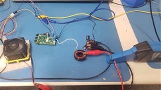
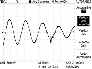
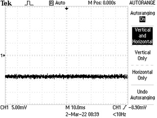
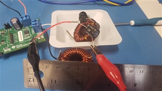
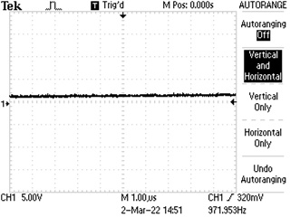
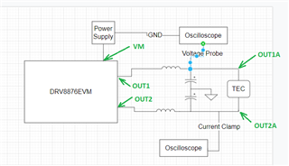
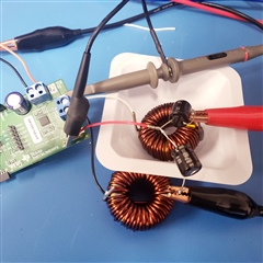
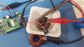
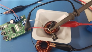
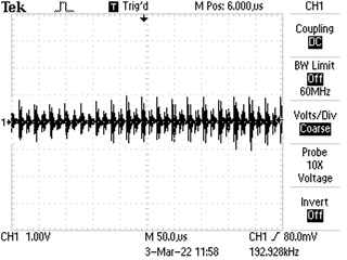
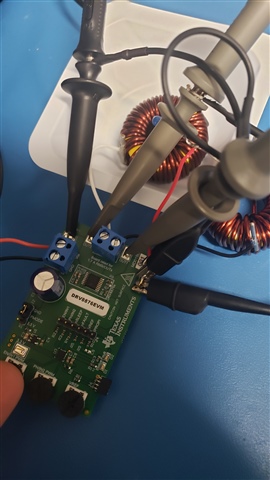
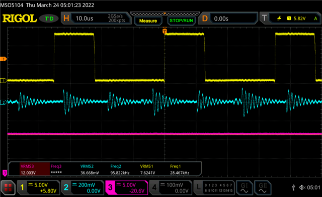
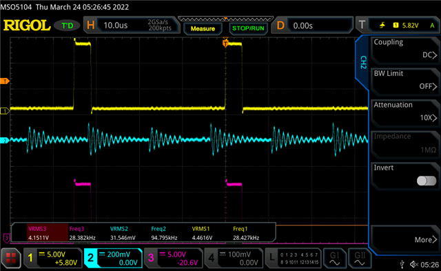
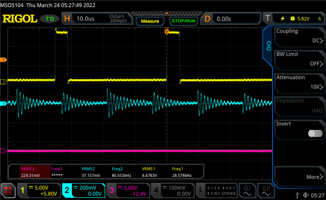
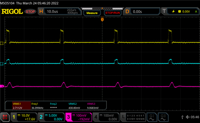
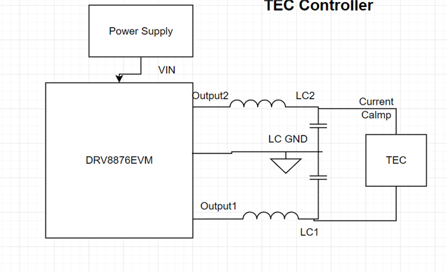
I just receive on of DRV8876EVM and it work fine but I have problem when I connect LC circuit to it the fault light turns on.

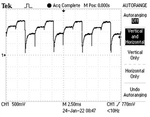
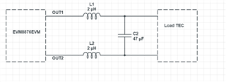
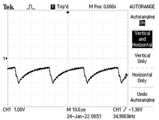
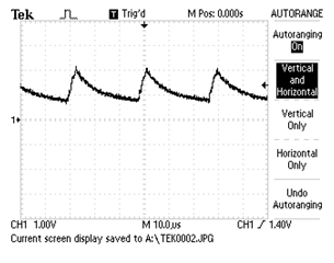
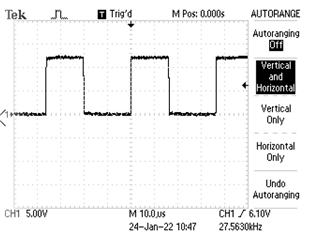
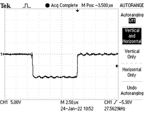
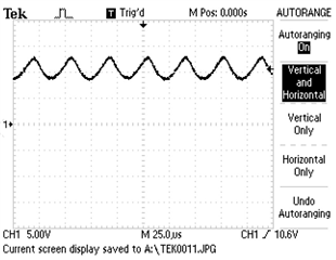
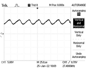
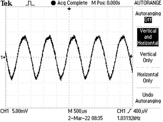
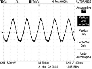
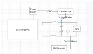
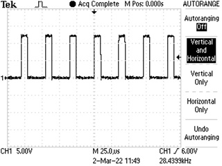
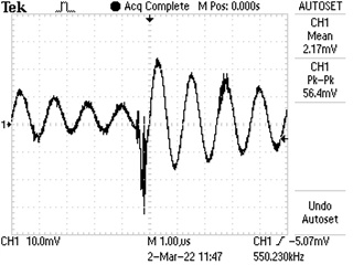
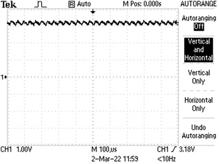
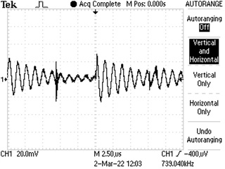
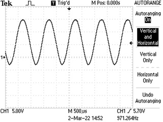
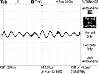
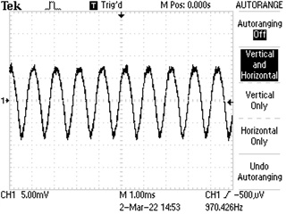
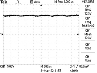
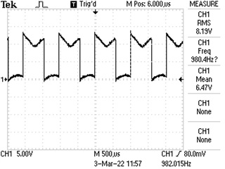
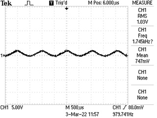
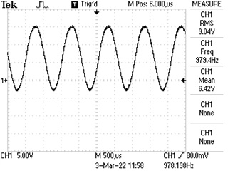
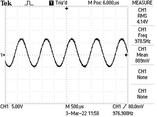
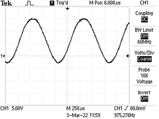
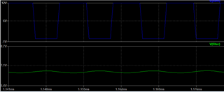
scope: we are trying to run TEC with this h bridge, but in order to smoot pwm we using inductor and capacitor as LC circuit.

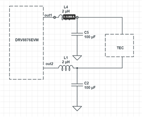
Base on my simulation, I should be able to smooth the 100khz pwm to sign way signal.

The cut of frequency I pick was around 707hz and inductor of 2uh and capacitor of 47uF

Please let me know if you need any other information.

  • Hi Amir,

    Can you share a Waveform showing the output voltages and nFAULT? Let's first determine what type of fault is triggering.

  • Hi Pablo,

    Thanks for the reply, I will be out office until Monday. I will send the waveform on Monday.

  • Amir,

    I will be waiting for your response.

  • Hi Pablo

    As I mentioned previously I am trying to run TEC and I need flatten the PWM as much as possible.

    I have tried different way to connect lC circuit below is the result

    When we have LC filter at both out1 and out2 and use two capacitor connected to GND (nFault turns on) as prev schematic

    This time I change circuit to below and I am not getting in nfault but no current is flowing and voltage is so low.

    Below is signal output without any load and no LC circuit

    Below No LC with Load 

    Thanks again for your help.

  • Amir,

    Have you tried a larger inductor and smaller cap?  For some example calculations specifically for TEC, please see section in following datasheet:

    https://www.ti.com/lit/ds/symlink/drv592.pdf

    Regards,

    Ryan

  • Hi Amir,

    Thanks for the information.

    One more question I forgot to ask: Is the nFAULT signal latching low? Do you have to reset the driver to resume operation? If so, this is most likely an OCP fault happening. To confirm, can you measure the output current?

    I think the LC filter is what is causing the fault since there is not fault when it is removed. I recommend playing around with the LC filter values. Try a lower capacitance first. I think the 100uF capacitor is causing large in-rush current which can be above the OCP threshold of the driver.

  • I accidently press solved problem can you remove it.

    I will go head and buy similar inductor and capacitor and try it again

    Also nFault will turn of as soon as I remove the LC filter no reset require.

    I have tried 47uF and even 20uF with 5uH inductor nothing works

    Also does DRV592 has any development board that I can test

    Thank you

  • I accidently press solved problem can you remove it.

  • Amir,

    The thread is still open.

    Also nFault will turn of as soon as I remove the LC filter no reset require.

    If you set the IMODE to Level 1 or 2, the driver will be in automatic retry so it will resume operation once the source of the OCP fault is removed.

    I have tried 47uF and even 20uF with 5uH inductor nothing works

    Can you try an even lower capacitance?

    Also does DRV592 has any development board that I can test

    Unfortunately, there is no EVM for this device

  • I will update this ticket as soon as I get the parts, thanks for the help

  • I just found 22uH and 4.7uF capacitor (connected capacitor to GND as circuit1) and it works in one direction but not the other. Nfault will not turn off until I reset power and only happen when I reverse direction.

    Also I found below:

    on out1 which is pulling 2A when I disconnect and reconnect load or reset Vref  the good side doesnt work any  more until I reset power supply, or turn of PWM I turn on slowly back on

    Below is without load which work perfectly

    Below is with load and is working, but as soon as you reset Vref or remove load nfault turns on

    I already order same10uH so I will have it next week. 

  • Hi Amir,

    I just found 22uH and 4.7uF capacitor (connected capacitor to GND as circuit1) and it works in one direction but not the other. Nfault will not turn off until I reset power and only happen when I reverse direction.

    This most likely means the motor is drawing more current in the reverse direction. This can be common in some motors and is caused by the construction of the motor. But at least you were able to get rid of the fault on one direction. Lowering the capacitor even more can help remove the fault in both directions.

    on out1 which is pulling 2A when I disconnect and reconnect load or reset Vref  the good side doesnt work any  more until I reset power supply, or turn of PWM I turn on slowly back on

    Most likely you are very near the OCP threshold and this caused a sudden large voltage transient at the output which caused the OCP fault.

    Please let us know once you get the new LC components and try lower capacitance.

  • Hi Pablo,

    I just received 10uH and 10uF unfortunately same issue , the nfault turns on both direction and out put. i

  •  Hi Amir,

    I think 10uF may still be too much capacitance. 

    Can you do one more thing if you haven't yet. Can you double double check your filter with the equations in page 10 of the datassheet below. In specific, check that the current ripple and voltage ripple are not too large given the LC filter and frequency.

    https://www.ti.com/lit/ds/symlink/drv592.pdf

  • Hi Pablo,

    Base on this equation Vm need more than Vtec otherwise ripple current will be zero

    I have tried 7V TEC but only 250mA current going through

    if I calculate for 7V TEC here is my result

    (12-7)*0.5*(1/400khz)/10e-6 = > 0.625 A  ripple current  and ripple voltage on 10uf is 27.344mV

    with 12V tec ripple current is zero and ripple voltage is 46.87mV

    How do you determine what value cause nfault. 

    Thanks gain for the help

  • Hi Amir,

    In your equation above, you are using 400kHz as the switching frequency. The DRV8876 has an abs max pwm frequency of 100kHz. If you redo the current ripple equation with 100kHz, you'll get a current ripple of 2.5A which can definitely trigger OCP. 

    To minimize the ripple, you have to increase the inductance.

    I think the LC filter is causing large current ripples which are causing the OCP fault to be triggered. I recommend playing around with the LC values to minimize the ripples as much as you can. I know there is a tradeoff between ripple and LC attenuation point. You'll have to make a judgement as to what is more important.

    Another option, if you need higher switching frequency and current is to use a driver like the DRV8412 (6-A; 70V; 500kHz) or the DRV8432 (12-A; 70V; 500kHz).

  • Hi Pablo

    No 100khz will for me but If I want keep ripple lower than 500mA then I have to user inductor larger than 50uH.

    I will go head and order some large inductors and see what happen.

    (12-7)*0.5*(1/100khz)/50e-6 = > 0.625 A 

    Thanks again for support

  • Amir,

    Sounds like a plan. Let me know what results you're getting with the higher inductance.

  • Hi Pablo,

    I was able to kind make it work with 68uH and 1uF but  still nfault turns on lower duty cycles. Main issue now TEC only able to pull 500mA which is not enough to heat device.  Also I tired to look at the output on oscilloscope to see if even LC circuit is flatting the signal (kinda sign wave)  and is not.

    I do not think this chip is good option to run TEC, do you have any other suggestion.

    Thank you 

  • Hi Amir,

    Thanks for the update.

    Please read this FAQ on driving TEC elements with motor drivers. This FAQ has useful information on how to best choose a motor driver based on your needs.

    Please let me know if you have further questions on any of the parts listed on the FAQ.

  • Hi Amir,

    It looks like TEC element is a load of resistive type with some internal voltage and it should be quite easy to drive it, driver with LC filter and load resembles dc/dc buck converter. If you can answer a few question:

    - what current do you need to run through TEC element ?

    - do you need to run current in one direction or both ?

    - what is TEC resistance when is not loaded and at room temperature ?

    - how do you drive DRV8876, is it with DRV8876EVM onboard MCU or with external signal generator ?

    - 68uH inductor - what is its resistance, what is its max. current ?

    - do you have a current probe, if so what type (it would be handy but not absolutely necessary) ?

    Regards,

    Grzegorz

  • Hi Grzegorz,

    thanks for the help. Below is answer to your questions:

    TEC we are currently using: CP303385H CUI

    1.  2.5-3A

    2. Yes, current on both direction

    3.  4 ohm base on datasheet

    4.I am currently using on board MCU on DRV8876EVm, but we are planning to control it with our microcontroller (Atmega2560)

    5. 68uH part number HCTI-68-7.7, and  rate for 7.7A and 30mohm

    6. No I do not have one but if need can buy it (I can ask my manager)

    Once more thanks for the help, please let me know if you have any questions.

    Thank you

  • Hi Amir,

    1. 3A probably will be too much for DRV8876, at 120C conductive losses alone would be 3x3x(0.5 + 0.5) = 9W. It is a lot of power to dissipate. With a properly designed 4-layer pcb you would be probably able to run DRV8876 at around 2A continuously.

    2. Then normal aluminium unipolar capacitors can not be used in LC filter (unless connected opposite in series - I have not checked such connection myself yet). The choice would be aluminium bipolar (need care about ripple current, temperature and life), MLCC or polyester/polypropylene caps.

    3. Then 12V might not be enough to get 3A, 15-18V would be more appropriate.

    4. I am not sure if you can run DRV8876EVM at 100kHz with onboard MCU without reprogramming it. Looking at all waveforms above we can see that frequency is around 30kHz. At 30kHz I would use 220uH-1mH inductor and cap/caps somewhere between 47-470uF at the beginning for trials.

    5. It looks OK, just its inductance is too low for 30kHz.

    6. That should not be a problem, circuit looks quite simple and probably you will be able to test it without current probe.

    I think if you want to evaluate driving TEC with DRV8876EVM board you would need either signal generator or MCU that can give 90-100kHz PWM signal or buy some inductor at least 220uH plus proper capacitors 47-470uF if you want to make trials at around 30kHz.

    For 3A current I would go for a driver with much lower Rdson and preferably higher max. frequency, the higher frequency the smaller inductors and capacitors are needed what makes design cheaper but usually a bit more difficult to make.

    Now the question is if you like to continue trials with DRV8876EVM? I think it would give you some experience and allow to design something more suitable for your needs. I would start with LC filter with 2 inductors and 2 caps, it seems to be simpler to understand, control and test.

    Regards,

    Grzegorz

  • Hi Grzegorz,

    Thanks for the quick replay. 

    1. 2A it should be more than enough for us. Yes we are planning to use 4layer board

    2. I am using ceramic capacitor (Since Pablo suggested)

    3. I agree 12V may  not be enough for 3A but that's my design criteria. 

    6. Will go head and buy one

    I like to continue working DRV8876EVm until I have some solid result so I can then move to board design. (If we have to we can connect external Microcontroller to program the DRV8876)

    So I will go head and order 250uH (ATCA-08-251M-H) and  100uF (ECA-1EEN101) capacitor and let you know the result.

    Just one question how are you calculating your L C for PWM signal. (I understand for LC F = 1/(2*PI()*SQRT(L*C)))

    Thanks 

  • Hi Amir,

    Inductor and capacitor look OK for trials, please just check if capacitor will not overheat during tests (you can connect two in parallel if needed).

    You gave proper equation for LC circuit resonance frequency. I do not have experience with driving TECs but I guess you need quite well filtered DC current/voltage to drive TEC. I would use equations used for DC/DC buck converters. First equation for current ripple where inductance should limit current ripple to a value that will not trigger OCP, you have mentioned such equation earlier. The second equation would be for output voltage ripple that would give necessary value of capacitance. The equations can be found in many DC/DC buck converters datasheets.

    I gave you just some LC values based on my experience with 200kHz DC/DC buck converter that should be good for your initial tests, then you can adjust LC values to your needs. I would use LC resonance frequency equation in case of problems with filter resonances but TEC is mainly a resistor and I guess there will be no such problems.

    I will explain later how I would try to drive load like TEC.

    Regards,

    Grzegorz

  • Hi Grzegorz,

    Thank you for your comments and replies on this thread.

    Amir,

    Keep us posted on your results. Thanks!

  • Hi Amir,

    I think to control voltage on TEC it would be good to keep one half-bridge low (LS Mosfet ON) while PWM switching another half-bridge with slow decay mode, probably it would be the most efficient way. I guess we would need also H-bridge Hi-Z state to turn TEC off completely. I think the easiest way to get all necessary states with DRV8876EVM board would be to use PH/EN mode.

    I would do the following steps:

    - set PMODE jumper to GND (PH/EN mode) while power, LC filter and TEC are disconnected,

    - power board up,

    - set VREF to around 3V with VREF potentiometer, it should give Itrip around 2A,

    - turn PH potentiometer completely counterclockwise,

    - set EN potentiometer to middle position,

    - check with an oscilloscope OUT terminals voltages, one should be 0V and another one should be PWM wave changing according to EN potentiometer settings,

    - power board down,

    - set EN potentiometer back to middle position,

    - connect to output terminals LC filter (2 inductors + 2 capacitors) with TEC,

    - power board up,

    - check with an oscilloscope voltages on OUT and TEC  terminals if they are correct,

    - to change current direction turn EN potentiometer completely counterclockwise to lower output voltage to 0 then turn PH potentiometer completely clockwise then adjust output voltage with EN potentiometer,

    - to go into SLEEP mode R4 probably would need to be disconnected, if to be done under load please start with low current and watch if VM does not rise to much.

    During loading the board please observe IC temperature and if it is to high disconnect power or turn VREF potentiometer to lower the max. current.

    All above is just my opinion and I might be wrong because I know just DRV8876EVM documentation.

    Regards,

    Grzegorz

  • Hi Grzegorz,

    Thanks for the update, I will have the parts next week and should be able to provide the result. 

  • Hi Grzegorz,

    I have tested based on requirement and it works. Never thought I need that big of inductor to run this TEC. I really appreciated your help, just when ever you had time I will be appreciated if you can explain to me how to did come with these inductors and capacitor. 

    Below is the result.

    No Load one side:

    The other side

    Below picture are with current probe with 100mA per 1 mV

    Lower PWM

  • Hi Amir,

    I am glad you got some promising results and thanks for posting waveforms. Unfortunately the waveforms may indicate some possible problems. The second waveform shows some ringing, it would be good to find what is its max. amplitude. Third and fourth show probably LC filter resonance at resonance frequency.

    Could you share a circuit diagram of connections between board, LC filter components and TEC?

    Regards,

    Grzegorz

  • Hi Grzegorz,

    Below is diagram how I connect everything DRV8876EVM. Also recapture the voltage again without any load.

    Please let me know if you need any thing else.

    Inductor ATCA-08-251M-H (250uH 27mohm)

    Capacitor ECA-1HEN470 (47uF 20% 50V )

    Thanks

    Setup

    Voltage Probe (Between GND and Each output)

    No Load No LC (DRV8876EVM output) 


    With LC filter no Load

  • Hi Amir,

    On the second and last waveforms there are some oscillations caused probably by switching operation and long wires, their amplitude is not very large and I guess they should not cause any problems. The third one shows quite well filtered DC voltage.

    You can get more precise measurements by connecting oscilloscope probe grounding cable to metal bar in the right bottom corner of DRV8876EVM board. The shorter grounding cable the better.

    Please connect the GND point of both capacitors directly to that bar or with a short wire (no longer than lets say 3-5 cm)

    I am only worrying about possible LC filter resonance. Could you make the following measurements when TEC current is a sinusoid at around 1kHz (like on previous waveforms):

    1/ VM voltage to GND

    2/ both outputs at board terminals to GND

    3/ both outputs at capacitors to GND.

    Oscilloscope probe grounded to above mentioned GND bar, timebase 1us, 5V per division. It would be ideal if you could make these measurements together with current probe measurements.

    Regards,

    Grzegorz

  • Hi Grzegorz,

    I update the setup base on your guide line, below is the graph for each just didn't know what do you mean by VM.

    Two alligators go to oscilloscope.  every cable is around 5cm, I couldn't go smaller since the inductors are so big and do not want short anything.

    Please let me know if you need any other measurement. 

    With Load:

    1us per div 

    Other side 

    To ground of capacitor (Do you still want this with 5V/div)

    Current probe

  • Hi Amir,

    The setup looks now much better. By VM I meant power supply voltage at EVM board terminals. I placed all measurement points at your drawing.

    If you could measure all these 5 points against GND bar when TEC current is sinusoidal at around 1kHz (like in your previous post). Please, do not use "Autoranging", set manually the following settings Timebase 500us, 5V per division (if voltage is low please change it to 1V or 100mV per division), make sure oscilloscope channel is DC coupled (Settings DC/AC/GND).

    If you have oscilloscope probe like this one for an example

    https://www.tme.eu/pl/en/details/ge.1521/probes-for-oscilloscopes-and-scopometers/elditest/  please use it, at your picture you use red and black cables with crocodile clips to connect oscilloscope, they can pick a lot of noise.

    If you have dual channel oscilloscope please use one channel for voltage measurement (all those 5 points) and the second one for TEC current measurement, you can set that channel to 10mV per division.

    Please, sign all waveforms (VM, OUT1 etc.)

    I just noticed I asked you for 1us timebase in my previous post, I apologize it was my mistake, I meant 1ms but 500us should be better.

    Regards,

    Grzegorz

  • Hi Amir,

    Sinusoidal TEC currrent and caps voltages look like LC filter resonance. We will try to find its source and limit its amplitude. The third waveform from the top (from your last post) shows voltage of around 6.4V rms what gives capacitor ripple current of around 1-1.8A, that is much higher than its rated ripple current. Please, monitor temperature of capacitors, they may get hot and even explode. If they are getting hot, please try to add more of these caps in parellel, that may help to limit possible resonance.

    Regards,

    Grzegorz

  • Hi Grzegorz,

    Thanks again for your comment. Actual capacitor is warm but not too hot but I will add too cap in parallel to reduce chance.

    Below is the measurements.(unfortunately my scope channel two is not working and only could get your one channel)

    Please let me know if you need more measurement. (if even help I can setup live meeting if you have time)

    Setup:

    VM (is not very clean but is under load)

    At Out 1

    Out 2

    At capacitor ground 

    out1A (Close to LC filter)

    Out1B (Close to LC)

    Out1A close to TEC

    Current Probe

  • Hi Amir,

    Thanks for all those waveforms, please give me some 1-2 days to think it over. In the meantime could you measure EN/IN1, PH/IN2 and VREF voltages at the same conditions as last waveforms were taken. You can find them on connector in the middle of EVM board. It is strange that PWM wave at OUT1 has frequency 1kHz instead of 30kHz, DRV8876 might be in current regulation mode.

    Regards,

    Grzegorz

  • Hi  Grzegorz,

    Thank for the quick reply. Below is the measurement your requested. 

    EN/IN1 = 3.295V
    PH/IN2 = 0V
    Sleep= 3.295V
    Nfault = 3.295V
    Vref = 2.749V
    Ipropi = 1.833V

    These I measure with fluke meter. Please let me know  if I can help in any way.

    Once more thanks for you help.

    Thanks

    Amir 

  • Hi Amir,

    Lets start with last waveforms.

    1/ VM looks OK, its max. value is around 12.5V and min. value is around 12V

    2/ Voltage on OUT1 looks strange probably because of high voltage drop caused by Rdson and OUT1 current which depends on LC filter and TEC. Minimum OUT1 voltage is around 9.5V what gives 2.5V peak voltage drop, it is a lot.

    3/ Voltage on OUT2 is caused by voltage drop on LS Mosfet Rdson, its max. value is around 2V, again it is a lot.

    4/ Voltage on capacitor ground, it is some noise picked up by red ground wire and grounding cable of oscilloscope probe

    5 and 7/ OUT1A voltage, its max. value is 15V (more than VM max at 12.5V ) and has very nice sinusoidal shape, it suggests that LC filter is in resonance, not a big one but resonance. I think it is caused by OUT1 PWM frequency (1kHz) which is close to LC filter resonance frequency.

    Vref= 2.75V what gives current limit of around 1.8A, I estimated earlier that Rms current of capacitor is around 1-1.8A (1.4 - 2.5A peak) and TEC current is around 0.7A peak (it would be geometrical sum, so we can not just simply add these values), all that suggest that DRV8876 is working in current limit mode and it is causing that LC filter resonance. Additionally EN/IN1 is 3.295V, so probably PWM duty cycle is 100% and we can not see PWM of 30kHz at OUT1 and so on.

    8/ Current of TEC is sinusoidal and quite symmetrical with average value around 0V, what probably brings very low TEC efficiency.

    If you place current probe between OUT1 and inductor you may see a waveform similar to one on Figure 12 in datasheet below

    www.ti.com/.../drv8876.pdf

    I think you need to try to go out of LC filter resonance and possible current limit mode by:

    a/ Adjusting EN/IN1 potentiometer to lower EN/IN1 voltage so PWM of 30kHz will appear on OUT1 - the safest option

    b/ As above plus trying to lower/increase capacitance of capacitors what may bring possibility to work with a bit higher EN/IN1 voltage and PWM duty cycle (and TEC current)

    c/ As in point "a" plus increasing current limit with Vref potentiometer - possibility of DRV8876 overheating.

    Regards,

    Grzegorz

  • Hi Grzegorz,

    Thanks again for your detail response. I will go head and try your suggestion and send you the result, mean while   I was thinking instead of using LC filter with DRV8876, I use gate driver to control the H bridge and variable switching regulator to control power supply., like below diagram. Do you think this work better (I know is not very cost friendly)?

    This way I have not to worry about PWM any more. 

    I really appreciated your support.

    Thanks 

    Amir

  • Hi Amir,

    I think there is a good chance that it would work. You would still have an LC filter at the switching regulator and possible issues with regulator stability unless you go for a ready to use DC/DC converter module.

    Regards,

    Grzegorz

  • Amir,

    One question.  Are you using electrolytic capacitors (polarized) in your circuit?  I can't tell exactly from the picture, but seem like they may be.  

    Please use film or ceramic that are not polarized.  

    Regards,

    Ryan

  • Hi Ryan,

    Yes in this circuit I am using electrolytic capacitor, I will go head and change it to ceramic and send the data again. 

    Please let me know if you want me change any thing else.

    Thanks

  • Hi Ryan,

    Amir mentioned before that he was using electrolytic bi-polar capacitors  ECA-1HEN470

    https://www.mouser.pl/datasheet/2/315/ABA0000C1044-947503.pdf

    I think they should be OK for trials, though rather not a for final design because of short life.

    Regards,

    Grzegorz

  • Amir,

    Is there any update on this?  

    Regards,

    Ryan

  • Hi Ryan,

    Digi key mess my order on ceramic capacitors(ground shipping instead of air), should have something by end of this week, sorry about that. 

    I only have Electrolytic capacitor that large. 

    Thank you 

  • Amir,

    Appreciate the update.  Will hold.

    Regards,

    Ryan

  • Hi Ryan,

    I received my ceramic capacitor, as before  the the current very low, also LC filter did not filter the PWM as you can see on second result.

    1. No Load   Ch1: output2  Ch2: output1 Ch3: Vin


    2. No Load with LC filter:  Ch1: output2  Ch2: output1 Ch3: Vin

    2. No Load with LC filter:  Ch1: LC2   Ch2: LC1 Ch3: LC GND

    2. With Load with LC filter:  Ch1: LC2 Ch2: LC1 Ch3: Current Probe (1mV/ 100mA)

    Please let me know if you need more data.
    I purchase 22,10, and 4.7uF ceramic capacitor too. 

    Thanks

  • Amir,

    Sorry, I am little confused at where the measurements are being taken.  Can you please mark on diagram below?

    Regards,

    Ryan

  • Hi,

    See if this help 

    1. No Load   Ch1: output2  Ch2: output1 Ch3: Vin

    2. No Load with LC filter:  Ch1: output2  Ch2: output1 Ch3: Vin

    3. No Load with LC filter:  Ch1: LC2   Ch2: LC1 Ch3: LC GND

    4. With Load with LC filter:  Ch1: LC2 Ch2: LC1 Ch3: Current Probe (1mV/ 100mA)

    Please let me know if you need more information. 

    Thanks