This thread has been locked.

If you have a related question, please click the "Ask a related question" button in the top right corner. The newly created question will be automatically linked to this question.

DRV8316REVM: Testing Slew Rate, Active Demagnetization, and Cycle by Cycle Current Limiting

Part Number: DRV8316REVM
Other Parts Discussed in Thread: DRV8316

Hello, 

I have been evaluating this eval extensively for the past week and I have a few questions.

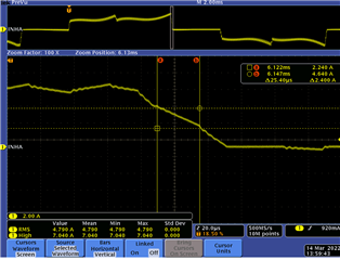
1) About the slew rate setting, the observed slew rates are quite different from the slew rate setting that is set. I see that only typical values are stated in the datasheet, so I am guessing there is quite a variation on how SR is achieved in the DRV8316. How much of this error is the DRV8316? Is this error vastly different between different DRV8316 batches or are they more or less deterministic? Is this motor dependent as well? We just want to isolate the fact that variation in this feature doesn't drastically affect motor performance. For reference here were the measured slew rates vs the set slew rates I have observed:

25V/us:  44.4V/us

50V/us: 46.2V/us

125V/us: 214.3V/us

200V/us: 342.9V/us

2) About active demagnetization, how do I go about testing/verifying that it is making a difference?

3) I am kind of confused by how cycle by cycle current limiting is implemented. Section 8.3.11 of the datasheet says that VREF is used for I/V converter as reference, but in 8.3.13, it says that AVDD is used as reference? If the former is true, how does current limiting work when the SOx output is dependent on the voltage at VREF/ILIM pin, which is compared to the VILIM set by that very same pin?

  • Also I am confused to how 8A translates to VREF/2 - 0.4V at ILIM.

  • Hi Jerome,

    1) Please be sure you are calculating from 20-80% of OUTx low to high voltage for slew rate. From looking at DRV8316 characterization data, there are some observations I noticed:

    • There is higher variation in higher output slew rates (i.e. 200 V/us) compared to lower slew rates (i.e. 25 V/us). 
    • The variation is a lot higher for slew rate switching from HIGH to LOW rather than LOW to HIGH. LOW to HIGH slew rates are on average under the typical spec, and HIGH to LOW slew rates are a bit higher than the typical specs on average. Your data falls in these min/max ranges for HIGH to LOW. 

    This likely varies device to device through process variation. This should not vary batch to batch. 

    2) You can test active demag by monitoring the body diode drop through the motor current switching. This E2E post can help identify how active demag works: https://e2e.ti.com/support/motor-drivers-group/motor-drivers/f/motor-drivers-forum/1003893/drv8316revm-how-to-use-active-demagnetization-on-drv8316revm

    Figure 8-32 is a simplified representation of how the body diode current can be measured. Here's an example of the body diode current conduction. During active demag, the LS MOSFET will be turned on so current flows through the FET rather than the body diode to save on power losses. 

    3) The I/V converter uses AVDD as the reference when comparing the realized phase current to the ILIM voltage applied. Think of CSAs / cycle-by-cycle current limit as a switch, either VREF is used as the source for the I/V converter (see figure 8-27), or ILIM is used a comparator threshold voltage (see figure 8-35). 

    This is why Equation 17 is referenced to AVDD --> the voltage realized from the internal SOA/SOB/SOC measurements is compared to the VILIM voltage. The current limit set is inversely proportional to the voltage range: 0A = AVDD/2, 8A = AVDD/2 - 0.4V. 

    Thanks,
    Aaron

  • 1) Yes I used the 20% to 80% for slew rate. Ok, this is interesting. We will take this information into account as we tweak slew rate. Since we are considering FOC, slew rate shouldn't matter as much so we were thinking of just applying the highest SR possible on the driver...

    2) Hmm, I looked at the phase voltage whenever body diodes should be conducting and the phase voltage was the same with or without AAR/ASR. I could not see the "-0.7V or VM+0.7V" the post was referring to. Either way, it seems that FOC might be used in our use-case so this feature may not be that big of a deal anyways.

    3) Ok this makes more sense as I forgot that you need to turn on current limit mode which will cause SOx to reference AVDD instead of the voltage at VREF/ILIM pin. I guess the equation still doesn't make sense to me because I don't know how 8A translates to AVDD/2 - 0.4 especially since there are different GAIN settings that would change that mapping? Shouldn't VILIM translate to AVDD/2 - GAIN * Ilim?

  • Hi Jerome,

    1) Slew rate has the main trade-off of optimizing EMI and thermal conduction losses. Higher slew rates will yield worse EMI performance, but minimize conduction and switching losses. FOC results in higher switching losses to produce sinusoidal current waveforms, so customers tend to use higher slew rate settings to minimize thermals in the DRV8316. 

    2) ASR and AAR is used for trapezoidal commutation, these features save power losses by turning on the LS FETs rather than the LS body diodes when commutating. You won't see the body diodes conduct in FOC since it uses synchronous rectification. Please reference this post for more info: https://e2e.ti.com/support/motor-drivers-group/motor-drivers/f/motor-drivers-forum/1003893/drv8316revm-how-to-use-active-demagnetization-on-drv8316revm

    3) Let me check and see how this equation is derived. The realized voltage is the average of the 3 currents multiplied by the GAIN (which may be in the units of A/V) to derive the voltage subtracted from VAVDD/2. 

    Thanks,
    Aaron