This thread has been locked.

If you have a related question, please click the "Ask a related question" button in the top right corner. The newly created question will be automatically linked to this question.

DRV8306: Kindly review the scheme

Part Number: DRV8306

Hi Ti Team,

Kindly review the attached scheme.

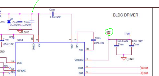
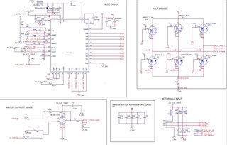
Prime Responsibility of the Driver is to drive the 120W BLDC Motor. DC Rail is 24V which is Coming from Boost Converter Output. Switching Frequency of the Boost Converter is 400kHz. scheme added Below

  • Hi Saneesh,

    I plan on looking over your schematic over the next few days and will try to provide feedback by the end of day on Wednesday.

    Regards,

    Anthony Lodi

  • Hi,

    Thanks for the feedback. Waiting for your response

    Best regards

    Saneesh

  • Hi Saneesh,

    Anthony will get you a reply tomorrow. 

    Thanks,
    Aaron

  • Hi Saneesh, 

    I will look over the schematic some more tomorrow, but I noticed you have a 2.2uF VM to VCP capacitor instead of the 1uF capacitor that is recommended in the datasheet. Is there a reason you are using a 2.2uF capacitor instead of the recommended value? 

    Additionally, in the schematic you show a 24V rail. Where is that coming from? Is it the same as VM (pointed to by the green arrow?) I don't see a net label on the VM connection, so I wasn't sure if it is the same source as the 24V rail.

    Regards,

    Anthony Lodi

  • Hi Saneesh,

    I Reviewed your layout and have the following feedback:

    1. Are you using differential hall elements or single-ended hall elements? I get the impression that you are using single-ended hall elements, in which case you will need to follow the instructions in section 8.1.1.2 of the datasheet to properly configure the HPx and HNx pins with some resistors.

    2. For the IDRIVE pin, I notice you chose to populate an 18kohm resistor to DVDD, which would result in an IDRIVE setting of 135mA/270mA source/sink current. The Qgd value of the MOSFET that you are using will be a big factor in deciding the appropriate IDRIVE setting, with the Vds MOSFET switch on time being equal to Qgd/IDRIVEP and the Vds MOSFET switch off time being equal to Qgd/IDRIVEN. Using an IDRIVE setting that is too high for the Qgd of the MOSFETs can cause undesirable EMI/ringing issues, so make sure you chose an appropriate IDRIVE setting. It is helpful to have the footprint available in the schematic to allow for adjusting the IDRIVE if you see that it needs to be lowered during testing. Most customers consider a 200ns/100ns rise/fall time as fast, and depending on the layout that switching speed may still lead to undesirable ringing issues during switching. I would recommend to start with an IDRIVE setting that would result in a 200ns/100ns switching time based on the MOSFET Qgd, and then ensure that you have the ability to reduce the IDRIVE setting to a lower value if needed if you see issues during testing with ringing during MOSFET switching. 

    3. The datasheet recommends a 1uF capacitor on DVDD, I would recommend switching out the 2.2uF capacitor with a 1uF capacitor. 

    4. I would recommend adding some bulk capacitance at the drains of each high side MOSFET so that there is some charge stored that can be used if there is a dip in the supply voltage. Additionally, small bypass capacitors located near the high side drains of the FETs can be beneficial in helping filter out high frequency noise on the supply. 

    5. The VM-VCP cap needs to be changed to 1uF. 

    6. Make sure your VM and VDRAIN are connected to the same net.

    Some additional resources that you may find helpful:

    System Design Considerations for High-Power Motor Driver Applications

    Best Practices for Board Layout of Motor Drivers

    I hope that helps!

    Regards,

    Anthony Lodi

  • Hi,

    Thanks for the immediate response. Below are My response

    1. VM and VDRAIN are connected to same NET
    2. 24V rail is Common for VM and Bridge circuit.
    3. I drive setting will fine tune as per your recommendation. I will share you the PCB  also for tour review once it is ready. 
    4. 4.7uF 1210 Package decoupling Capacitors are planned near to each of the arms of the bridge
    5. since the 24V Rail is coming from the Output of Boost Converter. Bulk capacitance across the boost Converter output is 250uF.  Are you telling that still I need to add add Bulk Capacitor near to the Bridge? we have added 20uF ceramic Capacitors near to the bridge to PCB Space and Height Constraint. is that Ok?

    Best regards

    Saneesh

  • Hi,

    I have two more  more Concern in the scheme.

    1. We are not using the I sense Protection  DRV8306. To disable this Current protection, I connected ISEN Pin to P_GND. is it right? 
    2. Top side FET Sources are connected to SHA, SHB and SHC. What about Bottom FETs?  I am Bit Confused here. 

    Best regards

    Saneesh

  • Hi Saneesh,

    Thanks for the clarifications!

    Even with the bulk capacitance at the output of the boost circuit, adding bulk capacitance near the half-bridges is beneficial to have local stored charge that is close to the MOSFETs ready to supply voltage to the MOSFETs if there is a dip for a brief duration of time on the supply. Based on the expected power of your motor during operation, a good starting point for bulk capacitance near the MOSFETs is 2uF per W.  

    Disabling the ISENSE feature by tying the ISEN pin to P_GND is the correct way to do it. 

    For the bottom FETs, the low side sources are not routed back to the motor driver. Instead, the driver uses PGND as the source reference for the low side MOSFETs (see below diagram).

    Regards,

    Anthony Lodi

  • Hi,

    Thanks for the response

    Most of My Queries Clarified

    Still one more is pending

    As per My design, Current sense resistor(R831) placed between Sources of the bottom MOSFETs and P_GND.  This Current sense resistor is to monitor the motor Current. Motor Current is monitored by the Microcontroller instead of DRV. In that Case I am not able to Connect the Sources of the Bottom MOSFETs to the DRV. Instead of source connection,  I connected P_GND to the ISEN pin to disable the DRV Current sense. whether this connection can cause any Ground Bounce due to presence Current sense resistor between Sources of bottom FETs and P_GND? 

    Best regards

    Saneesh

  • Hi Saneesh,

    I don't see any concern of additional ground bounce with the way you are implementing it. The only concern I have is that connecting ISENSE to PGND will effect the VDS monitoring for the low side MOSFETs. The low side MOSFET VDS monitoring is done with respect to ISENSE, and since ISENSE in your case is connected to GND, this results in the VDS monitoring to be monitoring the VDS drop of the low side MOSFET plus the drop across the sense resistor. This will result in the low side VDS OCP monitors to trip at a lower current than the high side VDS monitors. The VDS monitoring is used to help shut down the device in the case of high overcurrent events. The way this is implemented is a VDS threshold is set by the VDS pin, and if the voltage drop across the MOSFET exceeds that threshold then the VDS monitors will trip and shut down the DRV. The VDS monitoring trip current can be approximated by: Ids_trip = VDS_threshold/ Rds(on), but for your application the equation for the low side MOSFET trip current would be approximated by: Ids_trip = VDS_threshold/(Rds(on) x Rsense)

    The below image shows VDS monitoring using the ISEN pin connected to the LS MOSFET source

    The below image shows VDS monitoring with the configuration that you are wanting to implement:

    Notice now that the VDS monitoring now becomes Rds(on) + Rsense instead of simply Rds(on). As long as you are ok with this then I don't see any issues with connecting ISEN to PGND. 

    Regards,

    Anthony Lodi