This thread has been locked.

If you have a related question, please click the "Ask a related question" button in the top right corner. The newly created question will be automatically linked to this question.

DRV8306: Design Review

Part Number: DRV8306

Hi,

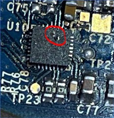
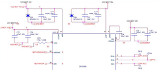
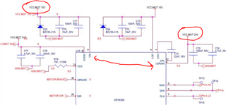
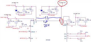
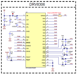
Please help me with a review of the below schematic for the DRV8306. Following are some of the changes that I have done already on board but then looking to see if there is something more that needs to be done.

  1. C77 is updated to 1uF
  2. R76 & R77 are update to 0E for now
  3. VCP is connected to VM using 1uF cap and D34, C72 & C73 are DNP
  4. HNx are removed from GND:MOT and currently floating

Along with a review could you also guide if:

  1. VM and VDRAIN can be connected to different BUS voltages? The reason I ask this is because I intend to drive a 24V motor and max. gate voltage for the selected FETs is 20V.
  2. nBRAKE, DIR, PWM & ENABLE would be able to tolerate a 5VDC input?

Thanks

Rishi

  • While carrying out the board bring-up below were some of my observations:

    1. When only VCC: MOT 15V was applied (HNA, HNB & HNC are floating and no hardware signals are applied)
      1. DVDD is found to be at 3.3VDC
      2. HPA & HPB are found to be at 3.3VDC
      3. HPC is found to be at 2.4VDC
      4. GLA, GLB & GLC are found to be at 0V
      5. GHA & GHB are found to be at 0.8V
      6. GHC is found to be fluctuating
      7. VCP is found to be at 25VDC
    2. Above values seemed okay and so VCC: MOT 15V was disconnected and only VCC: MOT 24V was applied (HNA, HNB & HNC are floating and no hardware signals are applied)
      1. Driver burnt after 4-5 seconds of power up. Below is the snip where the burnt region is marked.

  • Hi Rishi,

    I have concerns with this part of the schematic below:

    1) VM and VDRAIN are different voltages. VM is the supply for the DRV8306, and VDRAIN is a dedicated sense pin for the high-side MOSFET. These should not be different voltages. 

    2) There should be a 1uF cap connected from VM-VCP to generate the VCP voltage of VM+10V. VCP will be outputting current if it is reaching 25V, which VCP can only support up to 30mA max.

    3) Because there is more capacitance on VCP than VM, when the 15V rail is unpowered, it is likely VCP stays higher than VM over the 4-5 seconds. The damage you are seeing is ESD diode damage between VCP-VM if the damage is near those pins. 

    I would suggest fixing the schematic first before repowering the device because currently the schematic is not correct and will cause the part to not work correctly. You can review the DRV8306EVM schematic attached below to help show the correct connections needed to make the device work. 

    Thanks,
    Aaron