This thread has been locked.

If you have a related question, please click the "Ask a related question" button in the top right corner. The newly created question will be automatically linked to this question.

DRV8343S-Q1EVM: F280025 WITH DRV8343S SAMPLE PROJECT FOR SENSORLESS BLDC MOTOR CONTROL (MOST SUITABLE FOC OR TRAPEZODAL) ALGRATHRM

Part Number: DRV8343S-Q1EVM
Other Parts Discussed in Thread: TMS320F280025C, TMS320F280025, C2000WARE-MOTORCONTROL-SDK, DRV8323, LAUNCHXL-F280025C, INSTASPIN-BLDC, BOOSTXL-DRV8323RS, DAC128S085EVM, C2000WARE

Dear Aaron,

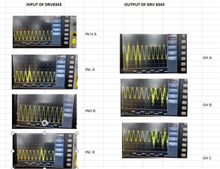
                   we are  interfaced drv8343 with msp430f5529c(non automotive) mcu with Trapezoidal-sensorless BLDC motors control algorithm , successfully tested on rig upto 9000 rpm  .

now we are trying to replace the c2000 family of TMS320280023 (automotive qualified) MCU with drv8343 driver ic ,

initially trying to interface tms320f280025c launch pad kit with DRV8343S evb board in going to use power module. 

i have taken as a reference universal_motorcontrol_lab_f28002x sample project trying to replace DRV8343S instead of DRV8323S, here both driver IC hardware abstraction layer is completely different . 

please let me know , which is the most suitable for tms320f280025 WITH DRV8343S Driver IC sample project for (demo source code for software) and hardware for the new development.

Please send supporting document and give your feed back ... 

Thanks .

Bhuvanesh.

  • Hi Bhuvanesh,

    I am forwarding your post to the C2000 team for more information on Universal motor control lab support. 

    Thanks,
    Aaron

  • Yes, you may refer to the Universal motor control lab, and you may try to follow Chapter 3 Building a Custom Board of the universal lab guide to interface the LaunchXL-F280025 to the DRV board, and change the device configuration codes and hardware setting parameters in the related files.

    C2000WARE-MOTORCONTROL-SDK: https://www.ti.com/tool/C2000WARE-MOTORCONTROL-SDK

    Universal Project and Lab User’s Guide: https://www.ti.com/lit/ug/spruj26/spruj26.pdf

  • Dear team,

                       i have interfaced (  developed source code , not connected driver ic with 280025c kit ) drv8343 driver ic with "universal_motorcontrol_lab_f28002x" project instead of drv8323 drv ic .

    as per the guide line "Motor Control SDK Universal Project and Lab document" trying to run the code Level 1 Incremental Build , without connecting drv8343 driver board (only 280025c launchpad kit ) for checking pwm ouput pulses and spi 

    i flashed the source code launchpad kit and observed flowing points 

    its not generate pwm pulse corresponding 6 pins !

    please let me know how can i check  pwm duty in debugging mode ?   

    if need to change any setting for "universal_motorcontrol_lab_f28002x" project ?  

    please refer same environment examples project for my reference   .


  • Please follow the guide to check the value of "motorVars_M1.faultMtrUse.all" if there is any fault, and try to fix these faults.

    You should connect the drv8343 in any build levels, and make sure that you configure the GPIO and SPI to interface and control drv8343 correctly.

  • I can attached following error in my understand not connected drv 8343 driver  board so that why showing undervoltage , but my intention without drv8343 board  to check pwm output pulses from mcu , henceforth connected power supply 3.3v from usb with tms320f280025c launchpad kit 

    i hope without drv8343 driver can able to check pwm pulses (duty) only , is it correct ?

  • Please check the value of "motorVars_M1.faultMtrUse.all", not the value of "motorVars_M1.faultMtrNow.all".

    Yes, as described in lab guide, you should run the  project in build level 1, and check the PWM output on the related pins on launchxl-F280025c.

  • we are trying to replace the c2000 family of TMS320280025C (automotive qualified) MCU with drv8343 driver ic (WITH SENSORELSS BLDC MOTOR) ,

     interfaced tms320f280025c launch pad kit with DRV8343S evb board power module are utilized. 

    i have interfaced (  developed source code , not connected driver ic with 280025c kit ) drv8343 driver ic with "universal_motorcontrol_lab_f28002x" project instead of drv8323 drv ic .

    as per the guide line "Motor Control SDK Universal Project and Lab document" trying to run the code Level 1 Incremental Build , without connecting drv8343 driver board (only 280025c launchpad kit ) for checking pwm ouput pulses and spi 

    now working on  As per the tabulation in yellow color  , have question on ,  is it support "FAST based senseless Foc" algorithm in BLDC motor ?   

    used as pre-define symbols "MOTOR1_FAST",  please let me know your feedback .

    above condition pwm output pulses not generate from MCU , but i can see spi output pulses .

    and also ,

    As per tabulation have mention in red color "Trapezoidal InstaSPIN-BLDC"  and pre defined symbol  "MOTOR1_ISBLDC".

    is it support senseless BLDC motor control algorithm?

    please let me know  below tabulation which one support (enable) motor control "Algorithms or
    Functions" and "Pre-Define Symbols" to drive the senseless BLDC motor with f280025c +drv8343s driver IC 

  • now working on  As per the tabulation in yellow color  , have question on ,  is it support "FAST based senseless Foc" algorithm in BLDC motor ?   

    used as pre-define symbols "MOTOR1_FAST",  please let me know your feedback .

    Yes, you can use the FAST based sensorless-FOC on three-phase BLDC or PMSM.

    is it support senseless BLDC motor control algorithm?

    Yes, it's sensorless trapezoidal control.

    please let me know  below tabulation which one support (enable) motor control "Algorithms or
    Functions" and "Pre-Define Symbols" to drive the senseless BLDC motor with f280025c +drv8343s driver IC 

    All of the sensorless based algorithm can be used on f280025c +drv8343s driver IC that includes FAST, ISBLDC, and eSMO as mentioned above. You may try to use the FAST that could be easy to spin a motor and achieve better performance.

  • We haven’t heard from you for a week, so we are assuming you were able to resolve your issue. Please let me know if you have any questions. We would like to close this thread if no any further questions. Thanks!

  • now i have interfaced drv8323S ( BBOSTXL-DRV8323RX) with f280025c launchpad kit  (LAUNCHXL-F280025C ) 

    trying to check the current and voltage adc offset value as per the document  , to debug the build level1   #define DMC_BUILDLEVEL  DMC_LEVEL_1

    but i have facing fault on current and voltage offset error ,

    please let me know your feed back,


    Also i could not read the default offset value of voltage and current as mention below,  

    Please let know your feed back .

  • Please take a look at the lab guide and follow it to connect the kits. Make sure that the related switches are set correctly on LAUNCHXL-F280025C, and the connection is as below shown in the lan guide.

    • For more details about the BOOSTXL-DRV8323RS, see the User's Guide for the EVM.
    • Make sure that the following items are completed as described below, and then connect the BOOSTXLDRV8323RS
    to J1/J3 and J4/J2 of the LAUNCHXL-F280025C as shown in Figure 2-7.
    – Populate C9, C10, and C11 with a 47nF capacitor.
    – Bend J3-29 and J3-30 of the LAUNCHXL-F280025C90 degrees so that they are not connected to the
    BOOSTXL-DRV8323RS as shown in Figure 2-5.
    – If using the DAC128S085EVM board, bend J5-42 of the LAUNCHXL-F280025C 90 degrees to avoid
    connecting that pin to the DAC128S085EVM board. This EVM board is only used for debugging purposes
    to monitor various software variables.
    – Use a jumper wire to connect J3-29 of the LAUNCHXL-F280025C to J3-11 of the BOOSTXL-DRV8323RS
    if the potentiometer functionality is desired to be used on the BOOSTXL-DRV8323RS for setting the
    reference speed.

    Universal Project and Lab User’s Guide: https://www.ti.com/lit/spruj26

  • As per the guide line configured and tried to initial offset value from voltage and current  , but not able to read correct offset value as per the reference (spruj26_Motor Control SDK Universal Project and Lab) document in (#define DMC_LEVEL_1     1   // Y 50% duty, offset calibration and verify phase shift)


    PLEASE LET ME KNOW IF I NEED TO ANY CHANGE  HARDWARE BOARD ?

    HOW CAN I GET EXAXT OFFSET VALUE FROM BUILD LEVEL1 ? 

     PLEASE LET ME KNOW YOUR FEED BACK (IS IT POSSIBLE PINK ME THROUGH WHATSUP. MY CONDUCT NUMBER +91-9003224712)

  • Seems like BOOSTXL-DRV8323RS is not connected with LAUNCHXL-F280025C correctly, please follow the guide and the instruction as mentioned above to set up the kits, may try to check the PWM output and ADC input voltage on the related pins on BOOSTXL-DRV8323RS with an oscilloscope.

    BTW, you need to add the dc-bus voltage to the BOOSTXL-DRV8323RS in build level 1 for offset calibration.

  • I have trying to interface f280025c launch pad kit with Boostxl drv8323rs also to monitor signal to interfaced DAC128S085EVM,

    connected dc bus voltage 12v to drv8323 evm and  also can red successfully 12v dc bus voltage as i mention below image   

    connected following connectors as below mention ,

    Populated a 47nF capacitor to C9, C10, and C11 for supporting InstaSPIN-FOC.

    Connected J4-4 to J4-18 using a jumper wire for connecting DRV_SCS to SPI_STE,

    Connected JA-2 to JB-2 using a jumper wire , 

    Disconnected J3-29, J3-30 to BOOSTXDRV8323RS, 

    Disconnected J5-42 to DAC128S085EVM

    i hope hardware connection  done as per the above guide .

    i was selected  MOTOR1_FAST algorithms under pre defined signal on BSXL8323RS_REVA 

    added the dc-bus voltage to the BOOSTXL-DRV8323RS in build level 1 for offset calibration, and without motor connection.

    if enabled pre defined signal CMD_POT_EN , can able to read the pot value from 0 to1025   

    but still i could not able to read the ADC voltage and current offset value , checked related pins on BOOSTXL-DRV8323RS with an oscilloscope not get any output.

  • Please follow the lab guide to run the project in build level 1, and don't change the default configuration to enable much more functions like CMD_POT_EN..., and don't need to connect the DAC128S085EVM for build level 1.

    Please make sure that the switches are set correctly as shown in lab guide as below also, especially the S2.

    • Install jumpers on JP1, JP2, JP3 and J101 for the power supply and debug JTAG. And jumpers on JP8 for the power supply of DAC128S board if used.

    • For S2, position the SEL1 (LEFT) switch UP (1) to route GPIO28 and GPIO29 to the BoosterPack connector, and position the SEL2 (RIGHT) switch UP (1) to rout GPIO16 and GPIO17 to the virtual COM port of the XDS110 debugger.
    • For S3, position the SEL1(LEFT) switch DOWN to pull GPIO24 low to logic 0, and position the SEL2(RIGHT) switch UP to pull GPIO32 high to logic 1 to put the F280025C into wait boot mode for reducing the risk of connectivity issues or a previous loaded code execution.
    • For S4, set S4 to DOWN (on), GPIO32 and GPIO33 are routed to the CAN transceiver to J14 CAN interface if the pre-define symbols "CMD_CAN_EN" is set in project properties.
    • For S5, position the SEL1(LEFT) switch DOWN to route GPIO44/37/43 to eQEP1 for the encoder interface on J12, and position the SEL2 (RIGHT) switch DOWN to route GPIO14/25/26 to eQEP2 for the Hall sensor interface on J13.
  • Thank you for your valuable feed back !!!!

    As per your feedback In build level 1 without motor condition now i can read successfully offset value of voltage and current , got pwm output in register value 50% also , i am wounding this flag  always showing  flagEnableRunAndIdentify = 0, but as per guide this flag should be change to high (1) 

    The systemVars.flagEnableSystem should be set to 1 after a fixed time, that means the offsets calibration has
    been done. The fault flags, motorVars_M1.faultMtrUse.all should be equal to 0.

     motorVars_M1.flagEnableRunAndIdentify to 1 SHOULD NOT HAPPEND in the Expressions window 

    when started build level 2 with motor connection also we can got same value , 

    please i need your feed back on this ? 

  •  i am wounding this flag  always showing  flagEnableRunAndIdentify = 0, but as per guide this flag should be change to high (1) 

    You need to set the lagEnableRunAndIdentify = 1 in the CCS debug window to start the motor in all  build levels.

  • Thank you for support Luo!!!!

    Now i stated to interface drv8343 driver ic with c2000(f280025c) mcu , i have updated corresponding register in function which is having drv8323 deiver ic .

    now can able build with out error . below mention as modified function 

    void DRV8343_readData(DRV8343_Handle handle, DRV8343_VARS_t *drv8343Vars) 

    void DRV8343_writeData(DRV8343_Handle handle, DRV8343_VARS_t *drv8343Vars)

    void drv8343_SPI_Write(DRV8343_Handle handle, const uint16_t regAddr, const uint16_t data)

    uint16_t drv8343_SPI_Read(DRV8343_Handle handle,const uint16_t regAddr)

    void DRV8343_setupSPI(DRV8343_Handle handle,DRV8343_VARS_t *drv8343Vars)

    I will try to read adc offset value and Vadc bus voltage in level1 build  but caould not able to read 12 DC bus voltage and offset value also ,

    attached image for your reference Please let me know your feed back on this  

  • Please follow the lab guide to change the configuration parameters and codes in hal.h and hal.c, to ensure the ADC and PWM are configured according to the board and the connection you did.

    And also, you need to change the hardware parameters for current and voltage sensing in user_mtr1.h according to the board.

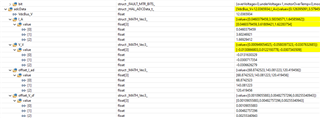
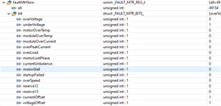
  •  successfully interfaced drv8343 with c2000(f280025c MCU)

    now i will trying to run the motor control SDK IN BUILD LEVEL 1 , I can read the default offset current value ,but i could not able to read offset voltage value.

    please let me know your feed back ,  what can i do? ..which parameter need to modification ? or else 

    is it  need to change vdc level ? 

  • Please make sure that ADC is configured correctly for voltage sensing, and the drv8343 is enabled by SPI and GPIO settings.

    To check the offset voltage, you need to add a right power supply for drv8343 evm board.

  • After populated 47nf capacitor i can successfully read the offset current voltage value in interfaced (f280025c with  RV8343) EVM board on BUILD LEVEL1.

    now i can run the BLDC motor on open loop in BUILD LEVEL2 capture Motor Phase Current and voltage Waveforms attached here ,

    here i can not able to capture exact the as mention "Motor Control SDK Universal Project" and Lab document output  

    I have attached phase voltage  and current output waveform for your reference, this following output wave form is it correct ?

    in my understand i can capture phase current output waveform is correct but   ,

    phase voltage and  angle (teta) output is not exact output so please let me know your feed back ?

    I want to tune the software on this required angle and phase voltage output , so please let me know on this your feed back ?

    how can i get exact angel output and phase voltage . 

    as i taking reference below  "Motor Control SDK Universal Project" document output .

  • I have attached phase voltage  and current output waveform for your reference, this following output wave form is it correct ?

    Not good. You may try to tune the Vd and Vq for running the motor with open-loop, and make the motor to run smoothly.

    I want to tune the software on this required angle and phase voltage output , so please let me know on this your feed back ?

    how can i get exact angel output and phase voltage . 

    You need to set the right motor parameters (Rs, Ls and Flux) to get the correct estimated angle. You can try to find the motor parameters in its datasheet or get the parameters from the motor's manufacturer

  • Hi luo

    now we are working working on instesd of f280025c - 80pin to (f280025-48 pin with drv8343 driver ic ) , i reused universal motor control project ,

    trying to build level1 to get the correct offset voltage and current value but now i can get correct offset value and vdc voltage value 

    but i can not read correct offset voltage . 

    i have changed 48 pin for below configuration and then select  48 pin corresponding adc channel MUX comparator

     PWM used gpio0 to gpio5 ,  instated of 80 pin only added gpio15 replaced into gpio5 remaining PWM GPIO pin same. (in this set source code i can run motor in EVM board)

    same setup file i can run motor successfully in launch xl f280025c-80 pin with drv8343 evm board but

    when i was used same source code our target board (f280025-48 pin) i could not read correct adc voltage offset value .

    please let me know your feedback on this.

    what is the difference between  280025c-80 pin and f280025-48 pin ?

    if i change pwm GPIO 5 INSTEADE OF GPIO15 shall i need to // XBAR-EPWM Config? in hal.h file .?

    f280025c -80 pin adc channal configration f280025 -48 pin adc channal configration
    //#define MTR1_IU_ADC_CH_NUM      ADC_CH_ADCIN11          // ADCA-A11*/C0
    //#define MTR1_IV_ADC_CH_NUM      ADC_CH_ADCIN4           // ADCC-A14/C4*
    //#define MTR1_IW_ADC_CH_NUM      ADC_CH_ADCIN7           // ADCC-A15/C7*
    //#define MTR1_VU_ADC_CH_NUM      ADC_CH_ADCIN6           // ADCA-A6*
    //#define MTR1_VV_ADC_CH_NUM      ADC_CH_ADCIN3           // ADCC-A3*/C5
    //#define MTR1_VW_ADC_CH_NUM      ADC_CH_ADCIN9           // ADCA-A2/C9*
    //#define MTR1_VDC_ADC_CH_NUM     ADC_CH_ADCIN6           // ADCC-C6*
    //#define MTR1_POT_ADC_CH_NUM     ADC_CH_ADCIN12          // ADCA-A12*/C1
    #define MTR1_IU_ADC_CH_NUM      ADC_CH_ADCIN15          // ADCA-A15/C7
    #define MTR1_IV_ADC_CH_NUM      ADC_CH_ADCIN0           // ADCC-A11/C0
    #define MTR1_IW_ADC_CH_NUM      ADC_CH_ADCIN2           // ADCC-A5/C2
    #define MTR1_VU_ADC_CH_NUM      ADC_CH_ADCIN0           // ADCA-A0/C15
    #define MTR1_VV_ADC_CH_NUM      ADC_CH_ADCIN3           // ADCC-A3*/C5
    #define MTR1_VW_ADC_CH_NUM      ADC_CH_ADCIN9           // ADCA-A2/C9*
    #define MTR1_VDC_ADC_CH_NUM     ADC_CH_ADCIN6           // ADCC-C6*
    #define MTR1_POT_ADC_CH_NUM     ADC_CH_ADCIN12          // ADCA-A12*/C1
  • what is the difference between  280025c-80 pin and f280025-48 pin ?

    It's no difference for the software of the Universal Motor Control Lab, just need to change the configuration codes accordingly. You can find the detailed difference in the datasheet. Make sure that the power supply and the VREFHI&VREFLO pins of the device are connected correctly.

    if i change pwm GPIO 5 INSTEADE OF GPIO15 shall i need to // XBAR-EPWM Config? in hal.h file .?

    No. Just need to configure the GPIO as PWM.

  • Hi Lue

    still i have faced issue for reading offset voltage , i have attached below image for your referance .

    we are changed GPIO as ePWM GPIO5 Instated of GPIO 15  which is having drv8323 with launch xl configuration in universal motor control project .

    drv8323 and 8343 bath V sense we are populated 47 nf  , we can read correct offset voltage and current value but  

    we are used our target board  Vsense capacitor 1.1 nf  

    is it need V sense capacitor 47nf ?  , please let me know your feedback. need clarification 


  • is it need V sense capacitor 47nf ?  , please let me know your feedback. need clarification 

    Yes, you need to use a larger capacitor like 33nF~68nF, and calculate the USER_M1_ADC_FULL_SCALE_VOLTAGE_V and USER_M1_VOLTAGE_FILTER_POLE_Hz according to the voltage sensing circuit.

    You can find the calculation example in the file Motor_Control_Parameters_Calculation.xlsx file at the folder below. 

    C:\ti\c2000\C2000Ware_MotorControl_SDK_<version>\solutions\universal_motorcontrol_lab\doc

  • Dear Luo

    we have still we are not get proper offset voltage value , we are changed hardware and software during debugging 

    here, i have attached  table for hardware and software changed during debugging and  issue was resolved but still not able to read the correct offset voltage value.

    here observed below ,

    WE CHANGED IN EVM FROM EXTERNAL CLOCK  100 MZH TO INTERNAL CLOCK  100MHZ

    when i was change pwm snitching frequency , that is not updating in expression window and registers  in corresponding period value  , always showing 15k frequency. period value   

    //! \brief Defines the Pulse Width Modulation (PWM) frequency, kHz.
    //!
    #define USER_M1_PWM_FREQ_kHz ((float32_t)(10.0f))

    #define USER_M1_PWM_TBPRD_NUM (uint16_t)(USER_SYSTEM_FREQ_MHz * 1000.0f / USER_M1_PWM_FREQ_kHz / 2.0f)

    . OUR TARGET BOARD USED INTERNAL CLOCK 100MHZ. below code 

    SAME THINK HAPPEND OUR TARGET BOARD ALSO BASED ON INPUT SWITCHING FRQ DID NOT UPDATE RGISTERS AND EXPRESSION WINDOW.

    // External 10 M INTERNAL
    // Set up PLL control and clock dividers
    // CPU Clock Frequency = 100MHz
    // PLLSYSCLK = 20MHz (XTAL_OSC) * 30 (IMULT) / (2 (REFDIV) * 3 (ODIV) * 1(SYSDIV))
    SysCtl_setClock(SYSCTL_OSCSRC_OSC1 | SYSCTL_IMULT(30) |
    SYSCTL_REFDIV(1) | SYSCTL_ODIV(3) |
    SYSCTL_SYSDIV(1) | SYSCTL_PLL_ENABLE |
    SYSCTL_DCC_BASE_0); 

    if i change USER_M1_PWM_FREQ_kHz shall i get changing period and value?

    how can i get offset voltage of  0.5 ,?

    please let me know your feedback, . if possible, can you share you mail id conduct number i will explain briefly . thank you

    how can verified pwm switching frequency in build level 1 ? 

  • Can you follow the lab user's guide to run the lab from the build level 1~4? And check the related outputs and measurement values?

    If you can get the right running result on the lab supporting kits, that means there are something wrong on your own hardware or the configuration codes.

    You may try to run the lab in build level 1, and change the codes as below in runMotor1OffsetsCalculation() in motor1_drive.c to check the ADC result for dc bus voltage and phase voltage.

    if(offsetCnt >= 2000) // Ignore the first 2000 times
    {
    offsetCnt = 2000;


  • Thank you for your feedback

    I HAVE ADDED AS PER YOUR GUILINE offsetCnt = 2000 , AFTER ADDING THIS VARIABLE NOE GET BLOW OFFSET VOLATGE ABD CURRENT VALUE 

    for(offsetCnt = 0; offsetCnt < 32000; offsetCnt++) //32000
    {
    // clear the ADC interrupt flag
    ADC_clearInterruptStatus(MTR1_ADC_INT_BASE, MTR1_ADC_INT_NUM);

    while(ADC_getInterruptStatus(MTR1_ADC_INT_BASE, MTR1_ADC_INT_NUM) == false);

    HAL_readMtr1ADCData(&obj->adcData);

    if(offsetCnt >= 2000) // Ignore the first 2000 times
    // if(offsetCnt = 2000) // Ignore the first 2000 times
    {
    offsetCnt = 2000;
    // Offsets in phase current sensing gAdcData

    IF RUN WITHOUT BREAK PIONTS WE GET BLOW VOLTAGE OFFSET AND CURRENT , DC BUS VOLTAGE 

    WHEN WE PUT A BREAK POINTS IN  FUNCTION runMotor1OffsetsCalculation()  line   
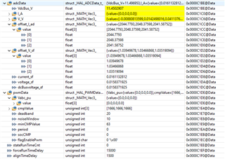
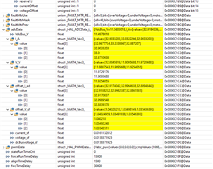
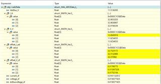
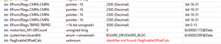
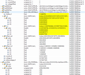
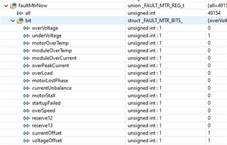
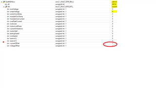
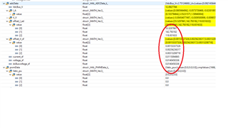
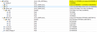
and  we,get the blow voltage and current offset value 

    here i am wondering offset voltage issue is based on software or hardware?  

    f280025c+ 80 pin with drv8343 launch pad source code midifed in hal.h and hacl.c  files which is corresponding to 48 pin f280025 mcu , only changed. A5 for  and gpio5 for  pwm3b.

    reused universal motor control project used external clock 100 mhz , we are modified. four target 28002c 48 pin into internal clock 100 mhz  

    we have done below configuration based in f280025 48 pin . STILL, WE ARE FACING VOLTAGE OFFSET ISSUE, PLEASE LET KNOW YOUR FEEDBACK . . 


    #define MTR1_IU_ADC_BASE ADCA_BASE        // ADCA-A15/C7
    #define MTR1_IV_ADC_BASE ADCC_BASE      // ADCC-A11/C0
    #define MTR1_IW_ADC_BASE ADCC_BASE // ADCC-A5/C2
    #define MTR1_VU_ADC_BASE ADCA_BASE // ADCA-A0/C15
    #define MTR1_VV_ADC_BASE ADCA_BASE // ADCC-A3*/C5
    #define MTR1_VW_ADC_BASE ADCC_BASE // ADCA-A2/C9*
    #define MTR1_VDC_ADC_BASE ADCC_BASE // ADCC-C6*
    #define MTR1_POT_ADC_BASE ADCA_BASE // ADCA-A12*/C1

    #define MTR1_IU_ADCRES_BASE ADCARESULT_BASE // ADCA-A15*/C7
    #define MTR1_IV_ADCRES_BASE ADCCRESULT_BASE // ADCC-A11/C0
    #define MTR1_IW_ADCRES_BASE ADCCRESULT_BASE // ADCC-A5/C2
    #define MTR1_VU_ADCRES_BASE ADCARESULT_BASE // ADCA-A0/C15
    #define MTR1_VV_ADCRES_BASE ADCARESULT_BASE // ADCC-A3*/C5
    #define MTR1_VW_ADCRES_BASE ADCCRESULT_BASE // ADCA-A2/C9*
    #define MTR1_VDC_ADCRES_BASE ADCCRESULT_BASE // ADCC-C6*
    #define MTR1_POT_ADCRES_BASE ADCARESULT_BASE // ADCA-A12*/C1

    #define MTR1_IU_ADC_CH_NUM ADC_CH_ADCIN15 // ADCA-A15/C7
    #define MTR1_IV_ADC_CH_NUM ADC_CH_ADCIN0 // ADCC-A11/C0
    #define MTR1_IW_ADC_CH_NUM ADC_CH_ADCIN2 // ADCC-A5/C2
    #define MTR1_VU_ADC_CH_NUM ADC_CH_ADCIN0 // ADCA-A0/C15
    #define MTR1_VV_ADC_CH_NUM ADC_CH_ADCIN3 // ADCC-A3*/C5
    #define MTR1_VW_ADC_CH_NUM ADC_CH_ADCIN9 // ADCA-A2/C9*
    #define MTR1_VDC_ADC_CH_NUM ADC_CH_ADCIN6 // ADCC-C6*
    #define MTR1_POT_ADC_CH_NUM ADC_CH_ADCIN12 // ADCA-A12*/C1

    #define MTR1_IU_ADC_SOC_NUM ADC_SOC_NUMBER1 // ADCA-A15/C7-SOC1-PPB1
    #define MTR1_IV_ADC_SOC_NUM ADC_SOC_NUMBER1 // ADCC-A11/C0 -SOC1-PPB1
    #define MTR1_IW_ADC_SOC_NUM ADC_SOC_NUMBER2 // ADCC-A5/C2 -SOC2-PPB2
    #define MTR1_VU_ADC_SOC_NUM ADC_SOC_NUMBER4 // ADCA-A0/C15 -SOC4
    #define MTR1_VV_ADC_SOC_NUM ADC_SOC_NUMBER5 // ADCC-A3*/C5 -SOC5
    #define MTR1_VW_ADC_SOC_NUM ADC_SOC_NUMBER5 // ADCA-A2/C9* -SOC5
    #define MTR1_VDC_ADC_SOC_NUM ADC_SOC_NUMBER6 // ADCC-C6* -SOC6
    #define MTR1_POT_ADC_SOC_NUM ADC_SOC_NUMBER6 // ADCA-A12*/C1 -SOC6

    #define MTR1_IU_ADC_PPB_NUM ADC_PPB_NUMBER1 // ADCA-A15/C7-SOC1-PPB1
    #define MTR1_IV_ADC_PPB_NUM ADC_PPB_NUMBER1 // ADCC-A11/C0 -SOC1-PPB1
    #define MTR1_IW_ADC_PPB_NUM ADC_PPB_NUMBER2 // ADCC-A5/C2- SOC2-PPB2

    // only for datalog and PWMDAC
    #define MTR1_IU_ADCRESLT MTR1_IU_ADCRES_BASE + ADC_O_RESULT1 // ADCA-A15/C7-SOC1
    #define MTR1_IV_ADCRESLT MTR1_IV_ADCRES_BASE + ADC_O_RESULT1 // ADCC-A11/C0 -SOC1
    #define MTR1_IW_ADCRESLT MTR1_IW_ADCRES_BASE + ADC_O_RESULT2 // ADCC-A5/C2- SOC2

    #define MTR1_VU_ADCRESLT MTR1_VU_ADCRES_BASE + ADC_O_RESULT4 // ADCA-A0/C15 -SOC4
    #define MTR1_VV_ADCRESLT MTR1_VV_ADCRES_BASE + ADC_O_RESULT5 // ADCC-A3*/C5 -SOC5
    #define MTR1_VW_ADCRESLT MTR1_VW_ADCRES_BASE + ADC_O_RESULT5 // ADCA-A2/C9* -SOC5
    #define MTR1_VDC_ADCRESLT MTR1_VDC_ADCRES_BASE + ADC_O_RESULT6 // ADCC-C6* -SOC6
    #define MTR1_POT_ADCRESLT MTR1_POT_ADCRES_BASE + ADC_O_RESULT6 // ADCA-A12* -SOC6

    //************************************************************* 80 & 48 PIN MAPPING ***********************************//

    //------------------------------------------------------------------------------
    // interrupt
    #define MTR1_PWM_INT_BASE MTR1_PWM_U_BASE // EPWM1

    #define MTR1_ADC_INT_BASE ADCC_BASE // ADCC-C6 -SOC6
    #define MTR1_ADC_INT_NUM ADC_INT_NUMBER1 // ADCC_INT1-SOC6
    #define MTR1_ADC_INT_SOC ADC_SOC_NUMBER6 // ADCC_INT1-SOC6

    #define MTR1_PIE_INT_NUM INT_ADCC1 // ADCC_INT1-SOC6
    #define MTR1_CPU_INT_NUM INTERRUPT_CPU_INT1 // ADCC_INT1-CPU_INT1
    #define MTR1_INT_ACK_GROUP INTERRUPT_ACK_GROUP1 // ADCC_INT1-CPU_INT1

    //------------------------------------------------------------------------------
    // CMPSS
    #define MTR1_IDC_CMPHP_SEL ASYSCTL_CMPHPMUX_SELECT_3 // CMPSS3-A14/C4*
    #define MTR1_IDC_CMPLP_SEL ASYSCTL_CMPLPMUX_SELECT_3 // CMPSS3-A14/C4*

    #define MTR1_IDC_CMPHP_MUX 4 // CMPSS3-A14/C4*
    #define MTR1_IDC_CMPLP_MUX 4 // CMPSS3-A14/C4*

    #define MTR1_IU_CMPHP_SEL ASYSCTL_CMPHPMUX_SELECT_1 // CMPSS1-C7, N/A
    #define MTR1_IU_CMPLP_SEL ASYSCTL_CMPLPMUX_SELECT_1 // CMPSS1-C7

    #define MTR1_IV_CMPHP_SEL ASYSCTL_CMPHPMUX_SELECT_1 // CMPSS1-A11
    #define MTR1_IV_CMPLP_SEL ASYSCTL_CMPLPMUX_SELECT_1 // CMPSS1-A11, N/A

    #define MTR1_IW_CMPHP_SEL ASYSCTL_CMPHPMUX_SELECT_3 // CMPSS3H-A5/C2*, N/A
    #define MTR1_IW_CMPLP_SEL ASYSCTL_CMPLPMUX_SELECT_3 // CMPSS3L-A5/C2*


    #define MTR1_IU_CMPHP_MUX 3          // CMPSS1-C7
    #define MTR1_IU_CMPLP_MUX 3          // CMPSS1-C7


    #define MTR1_IV_CMPHP_MUX 1         // CMPSS1-A11
    #define MTR1_IV_CMPLP_MUX 1           // CMPSS1-A11

    #define MTR1_IW_CMPHP_MUX 1              // CMPSS3H-A5/C2*, N/A
    #define MTR1_IW_CMPLP_MUX 1               // CMPSS3L-A5/C2*

    //#define MTR1_IV_CMPHP_MUX 4            // CMPSS3-C4
    //#define MTR1_IV_CMPLP_MUX 4               // CMPSS3-C4

    #define MTR1_CMPSS_DACH_VALUE 2048+1024+512
    #define MTR1_CMPSS_DACL_VALUE 2048-1024-512

    //------------------------------------------------------------------------------
    // XBAR-EPWM
    #define MTR1_XBAR_TRIP_ADDRL XBAR_O_TRIP7MUX0TO15CFG
    #define MTR1_XBAR_TRIP_ADDRH XBAR_O_TRIP7MUX16TO31CFG

    #define MTR1_IDC_XBAR_EPWM_MUX XBAR_EPWM_MUX05_CMPSS3_CTRIPL // CMPSS3-LP
    #define MTR1_IDC_XBAR_MUX XBAR_MUX05 // CMPSS3-LP

    #define MTR1_IU_XBAR_EPWM_MUX XBAR_EPWM_MUX00_CMPSS1_CTRIPH // CMPSS1-HP
    #define MTR1_IV_XBAR_EPWM_MUX XBAR_EPWM_MUX04_CMPSS3_CTRIPH_OR_L // CMPSS3-HP&LP
    #define MTR1_IW_XBAR_EPWM_MUX XBAR_EPWM_MUX01_CMPSS1_CTRIPL // CMPSS1-LP

    #define MTR1_IU_XBAR_MUX XBAR_MUX00 // CMPSS1-HP
    #define MTR1_IV_XBAR_MUX XBAR_MUX04 // CMPSS3-HP&LP
    #define MTR1_IW_XBAR_MUX XBAR_MUX01 // CMPSS1-LP

    #define MTR1_XBAR_INPUT1 XBAR_INPUT1
    #define MTR1_TZ_OSHT1 EPWM_TZ_SIGNAL_OSHT1

    #define MTR1_XBAR_TRIP XBAR_TRIP7
    #define MTR1_DCTRIPIN EPWM_DC_COMBINATIONAL_TRIPIN7

    #define MTR1_IU_XBAR_OUT_MUX XBAR_OUT_MUX00_CMPSS1_CTRIPOUTH // CMPSS1-HP
    #define MTR1_IV_XBAR_OUT_MUX XBAR_OUT_MUX04_CMPSS3_CTRIPOUTH_OR_L // CMPSS3-HP&LP
    #define MTR1_IW_XBAR_OUT_MUX XBAR_OUT_MUX01_CMPSS1_CTRIPOUTL // CMPSS1-LP

    //! \brief Defines the PWM deadband falling edge delay count (system clocks)
    #define MTR1_PWM_DBFED_CNT 5 // 50ns

    //! \brief Defines the PWM deadband rising edge delay count (system clocks)
    #define MTR1_PWM_DBRED_CNT 5 // 50ns

    // end of definition for site 1 (near emulator) on launchPad

  • here i am wondering offset voltage issue is based on software or hardware?  

    Please check if there is right PWM outputs on both input and output of the drv8343. Seems like the phase voltage sensing value is not correct during this offset calibration. The phase voltage should be the half of the dc bus voltage.

  • i verified muc ouput pwm , got 50 duty  less than 100mv pwm pin  ,also duty is not constant its varying.


  • Do you check the signals on the output of the drv8343? Any captured waveforms to show this? Do you configure the right GPIO to enable drv8343?

  • Dear Luo

    we have verified our target board output of drv8343 and captured wave form attached below .

    evn f280025c -80 pin with drv8343 gpio configuration working good,we can get correct offset voltage and current ,

    but same configuration used by our target board .

    checked pwm ouput of MCU and  driver output more are less same EVM and our target board , only different amplitude .

    still issue on same !!!

    if any suggestion? let me know    

  • These signals are not correct. The signals should be PWM waveform as shown in the lab user's guide. Any filter on these signals or oscilloscope channels?

    You have to check the hardware and software to ensure the PWM signals are right on both input and output of DRV8343 first by running the lab in build level 1. 

  • Hi Yanming 

    sorry for misleading ..

    still issue not rectified, we are verified software in build level 1 ,

    when we change pwm switching frequency (USER_M1_PWM_FREQ_kHz  ((float32_t)(10.0f)))  that should replicate on PWM register on below 

    here my observation always is showing motorVars_M1.ISRCount = 0 , when can ISRcount can increase ?


    if change  #define  that should e

  • Did you check if there is PWM output on the input and output of the gate driver again by changing the settings of the oscilloscope? And check the ADC result registers for dc bus and motor phase voltages

    here my observation always is showing motorVars_M1.ISRCount = 0 , when can ISRcount can increase ?

    After completed the offset calibration, the motorVars_M1.ISRCount will increase if can find the below code in motor1CtrlISR().

        motorVars_M1.ISRCount++;