Other Parts Discussed in Thread: DRV8872-Q1, DRV8872
Dear experts,
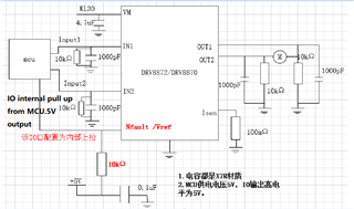
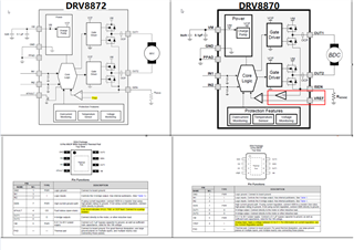
Due to supply shortage, customer is replacing DRV8872-Q1 by DRV8870 without changing any external circuit.. During debug DRV8870, there exist some issues and customer is focusing on PIN4 internal logic difference.
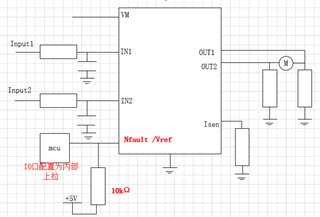
Referring to their schematic, do you have comments on the external configuration?
Problem statement:
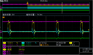
Under the same external circuit condition testing 8870. The abnormal driving problem is encountered during the process of raising the temperature from normal temperature to high(about 85 °C).
It can be seen from the test waveform that the waveforms of OUT1 and OUT2 are blocked under the condition of normal Vref of 5V, and the waveform interval time of 25us conforms to the internal overcurrent characteristics of the chip (actually, the input waveform of IN1 is 500ms pulse width). However, it can be seen from the actual current of CH4. There is no overcurrent.
CH1——out1,CH2——out2,CH3——PIN4(Vref),CH4——OUT1 current