


Dear Teams
We are working on project with DRV3255, there are some questions as below
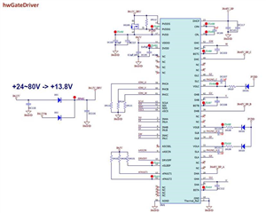
1. our circuit as below, in our design we don't need sleep function. so we connect nSleep pin to 5V
but in some case (ex: reboot), if 5V is build up faster than 48V, UV error (IC_STAT_3 = 0x55) shows up and can't be reset by IC_CTRL_1 bit0 even after all power is normal
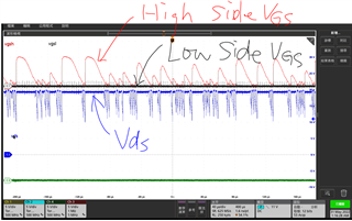
2. On our board test, when power up before SPI ENABLE_DRV=1b1, high side vgs will have abnormal output
this waveform we use 2n7002 signal level mosfet as gate drive test load, no motor or other load connected for inverter, and use differential probe for high side Vgs
we also found the abnormal high side Vgs will cause VGS_HA_L or VGS_HB_L or VGS_HC_L error (random)
We also double check with TI's EVB, after nSleep become high, there is some ripple at high side Vgs but not large enough to trigger error
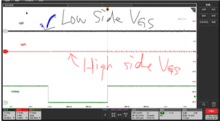
before enable drive we need to assure all gate driver output is high z or low
is there any setting error or linkage current at high side gate need to be take care?
best regards,
Albert
