This thread has been locked.

If you have a related question, please click the "Ask a related question" button in the top right corner. The newly created question will be automatically linked to this question.

DRV8301: Replace FETs with slower, higher Vgs(th) version - seeing a different problem now.

Part Number: DRV8301

Hi,

This thread is related to previous one:

https://e2e.ti.com/support/motor-drivers-group/motor-drivers/f/motor-drivers-forum/1108020/tms320f28069m-custom-board-design-failing-instaspin-lab-01c/4112659?tisearch=e2e-sitesearch&keymatch=%2520user%253A294039#4112659

Aaron Barerra is the TI Engineer most familiar with this design.

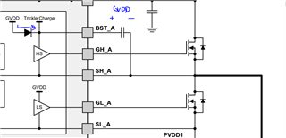
I replaced the BSO150N03MDG FETs with the AUIRFN8459TR. Same pin-out, dual FET pkg. The dimensions are slightly larger, but I could solder them right in where the previous FETs were.

The motor tries to turn in InstaSpin Lab 01b, but just fitfully moves a small fraction of a revolution. Here's a comparison of relevant characteristics:

FET Vgs(th)  Qg Rds(on) Qgd Ciss Id tr Comments
SUM110N06-3m9H 4V 200 nC 3.9mohm 45nC 15,800 pF 110A 160ns Used in Texas Instruments' DRV8301-69m kit, but no longer available.
AUIRFN8459TR 3V 40nC 4.8 mohm 14nC 2,250 pF 70A 55 ns Replaced BSO150n03MDG with these.
BSO150n03MDG 1.5V 12.6nC 20mohm 1.4nC 970 pF 9.3A 3.8 ns Original transistor that was experiencing "shoot-through."

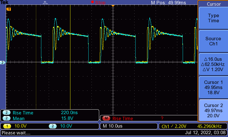
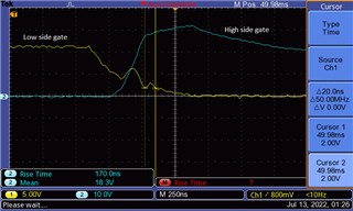
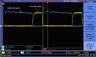
The new issue I'm seeing is illustrated by the figure below. The yellow trace is the High side gate, and the blue trace is the Low side gate of a pair (Q1 & Q2).

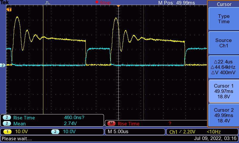
The high-side gate should be going up to about 34V, and it is, but all that ringing means it's only turned ON for a short period.

Any ideas what's happening here?

Thanks,

Dave

  • Hi Dave, 

    Thanks for reaching out over e2e md forum - 

    We will take a further look at your question early next week and aim to provide a response by Wednesday/Thursday timeframe 

    Best Regards, 
    Andrew 

  • Hello again Dave,

    Thanks for sharing the waveform, which is showing an enormous amount of ringing at the high side gate drive outputs. 

    Can you remind me again which gate drive current setting you are using, and if you are using any gate series resistors at the high side gate? 

    I have your previous schematic from back in December (EHP-FOC-10-sch.pdf), is this still accurate or is there a more updated schematic?

    Thanks,
    Aaron

  • Hi Aaron,

    I'll send you the most recent schematic & layout privately. Permanent changes made to the schematic since December are probably all communications related. Just remember to mentally replace the FETs with the AUIRFN8459TR. Also the gate resistors are 27 ohms. Dead time resistor is 40k (170ns). I haven't made these replacements on the schematic yet, since I'm not at all certain whether they'll be lasting. The gate current is set to 0.25A. Do you think the ringing might be related to the bootstrap caps? Either high side FETs being turned on first, not allowing caps to charge, or cap values too low?

    Thanks,

    Dave

  • Hi Dave, 

    Thanks for sharing. 

    Can you share what the switch node SH_x is doing in this condition as well? I want to confirm if this is real ringing across Vgs, or if the ringing is coming from the switch node. 

    Does this happen when there is no motor, or only when the motor is connected?

    Could you try lowering the gate resistors down to a smaller value, like 5-10ohms, to see if the waveforms improve? 

    Thanks,
    Aaron

  • Hi Aaron,

    I've attached some scope captures of switch nodes B & C. Looks like a lot of ringing there too. A looks pretty much the same as B, but C is much lower amplitude than either of them, but only when the motor is not present.

    Yellow trace is switch node B, blue is C, in both captures.

    I'll lower the gate resistors presently.

    Thanks,

    Dave

  • Hi Dave,

    This switch node ringing is likely oscillation due to source inductance or fast slew rate across the VDS of the MOSFET. 

    There are a few main ways to reduce this oscillation:

    1) Reducing gate drive current (min gate current setting and/or larger gate resistor) (resource)

    2) RC snubbers implemented across drain-source in parallel with each FET (resource)

    Unfortunately I think a major setback in this is that even these dual N-type MOSFET packages make it difficult to route in a half-bridge configuration, so there could still be switch node inductance between the two paths, especially at higher currents and faster VDS slew rates. Since there are not footprints for RC snubbers across the drain-source, our best bet would need to be to reduce the gate drive current further in order to dampen the switch-node oscillations and reduce the ringing at the gate. 

    Can you actually try to increase the gate resistors further, say 50-80 ohms? If the RC time constant of turning on the gate becomes too slow to the point where there both FETs could be on simultaneously (and cause shoot through), could you increase the dead time resistor to a much higher value, like 500ns?

    Also, as a final sanity check, make sure the low-side FETs turn on first before the high-side FETs in lab 1 so that the bootstrap caps can charge sufficiently. 

    Thanks,
    Aaron

  • Hi Aaron,

    I changed the gate resistors to 56 ohms. The ringing appears to be a lot less, but the high side gate signal drops to less than the required Vgs threshold (3V from gate to source) right after the first peak of overshoot, and stays there. The high side FET turns on (i.e. stays above 27V) for maybe 0.7us, not accounting for any hysteresis. Out of 22.2us, that's a duty cycle of about 3%. Dead time is still 170ns. Looks like I could adjust it to a lower value since right now the overlap (both FETs ON) is only about 20ns. Here are a couple pictures:

    I can't currently tell whether the high-side or low-side FET is turning on first. On startup, I've got the scope trigger set to normal, rising edge, and waiting for a single trigger (trigger level set to 0.8V), but it always seems to catch the first (?) pulse right in the middle. Sometimes the "first" one is the high-side gate sometimes the low-side.

    Thanks,

    Dave

  • Hi Aaron,

    At one end of each of the bootstrap caps are the actual phase voltages (PA, PB, PC) used to drive the motor coils. At the other ends are the bootstrap voltages (BST_A, BST_B, BST_C). These are identical in shape to the phase voltage, but raised up by 10Vdc. Not sure what to expect here, but is 10V of offset too little? By the way, this offset is present as soon as I start running the program - there are no signals going to the FET gates. It must be in one of the initialize routines. Is the DRV8301 adding that 10V as a result of an SPI instruction?

    Thanks,

    Dave

  • At one end of each of the bootstrap caps are the actual phase voltages (PA, PB, PC) used to drive the motor coils. At the other ends are the bootstrap voltages (BST_A, BST_B, BST_C). These are identical in shape to the phase voltage, but raised up by 10Vdc. Not sure what to expect here, but is 10V of offset too little?

    Hi Dave,

    This behavior is normal, GVDD (which is ~10V) charges up the bootstrap caps to SH_x + GVDD (minus the diode). This should happen once the LS FETs are turned on so that the bootstrap caps will charge. This is normal  bootstrap architecture  behavior and is not a SPI instruction. 

    Out of 22.2us, that's a duty cycle of about 3%. Dead time is still 170ns. Looks like I could adjust it to a lower value since right now the overlap (both FETs ON) is only about 20ns.

    Shouldn't the duty cycle at the offset calibration be 50%? 

    I can't currently tell whether the high-side or low-side FET is turning on first. On startup, I've got the scope trigger set to normal, rising edge, and waiting for a single trigger (trigger level set to 0.8V), but it always seems to catch the first (?) pulse right in the middle. Sometimes the "first" one is the high-side gate sometimes the low-side

    This is an issue we have seen before with a previous customer, where something in the firmware can cause the LS FET or the HS FET to turn on first. I don't know how open you are to modifying the firmware, but I have some email correspondence that talks about how to do this. This may contribute to the root cause of the problem, I can share this offline with you if you'd like. 

    Thanks,
    Aaron

  • Hi Aaron,

    Shouldn't the duty cycle at the offset calibration be 50%? 

    My point exactly. The Vgs(th) for this FET is 3V. The High-side FET should turn on at 3V + 24V. The base is only at that voltage or above for about 0.7us. The vast majority of its time "high" is spent at voltages well below the turn-on threshold.

    This behavior is normal, GVDD (which is ~10V) charges up the bootstrap caps to SH_x + GVDD (minus the diode). This should happen once the LS FETs are turned on so that the bootstrap caps will charge.

    It is happening well before any transistors are turned on. That's what I thought was weird about it.The labs for InstaSpin require that you start the program with the "Resume" button. There's some initialization that goes on, then the code waits for the user to change gMotorVars.Flag_enableSys and gMotorVars.Flag_Run_Identify to TRUE. Then signals are sent to the FETs, but supposedly not before.

    But in this case, as soon as I press the Resume button in Code Composer, the bootstrap caps are charged. Before that, they are not. If there were some other path to ground that allowed the caps to charge, it would be present as soon as I applied power (I would think). Could the low side FETs be getting turned on as part of the initialization?

    I can share this offline with you if you'd like

    I would love to see that.

    Thanks,

    Dave

  • Hi Dave,

    I reached out to you over PM so we can discuss over email and work with the C2000 team to determine why lab 1 is <50% duty cycle for calibration. 

    Thanks,
    Aaron

  • We have resolved this over email, closing this thread out. The resolution was the optimization settings (set to level 2) were optimizing out parts of the InstaSPIN-FOC firmware, the optimization level should be set to level 0. 

    Thanks,
    Aaron