


In the DRV8328 and DRV8329 gate driver devices, the external MOSFET’s drain-to-source voltage (VDS) slew rate will be dependent on the rate at which the gate of the external MOSFETs is controlled. The pull-up/pull-down strength of these gate drivers are fixed internally, hence the slew rate of each gate voltage can be controlled with an external series gate resistor. In some applications, the gate charge of the MOSFET, which is the load on gate driver device, is significantly larger than the gate driver peak output current capability. In such applications, external gate resistors can limit the peak output current of the gate driver. External gate resistors are also used to dampen ringing and noise.
The specific parameters of the MOSFET, system voltage, and board parasitics will all affect the final VDS slew rate, so generally selecting an optimal value or configuration of external gate resistor is an iterative process. To help calculate the approximate gate resistor values with +/-30% accuracy, use the BLDC Gate Resistor Calculator.
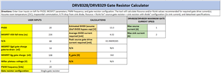
Figure 1 - Gate Resistor Calculator tool
To lower the gate drive current, a series resistor RGATE can be placed on the gate drive outputs to control the current for the source and sink current paths. A single gate resistor will have the same gate path for source and sink gate current, so larger RGATE values will yield similar SHx slew rates. Note that gate drive current varies by PVDD voltage, junction temperature, and process variation of the device.
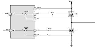
Figure 2 - Gate driver outputs with series resistors
Typically, it is recommended to have the sink current be twice the source current to implement a strong pulldown from gate to the source to ensure the MOSFET stays off while the opposite FET is switching. This can be implemented discretely by providing a separate path through a resistor for the source and sink currents by placing a diode and sink resistor (RSINK) in parallel to the source resistor (RSOURCE). Using the same value of source and sink resistors results in half the equivalent resistance for the sink path. This yields twice the gate drive sink current compared to the source current, and SHx will slew twice as fast when turning off the MOSFET.
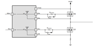
Figure 3 - Gate driver outputs with separate source and sink current paths
