This thread has been locked.

If you have a related question, please click the "Ask a related question" button in the top right corner. The newly created question will be automatically linked to this question.

DRV8908-Q1 OLD fault

Other Parts Discussed in Thread: DRV8908-Q1, STRIKE

hi , chips

  I have a question about drv8908-q1.   Could you help me solve the question, thank you.

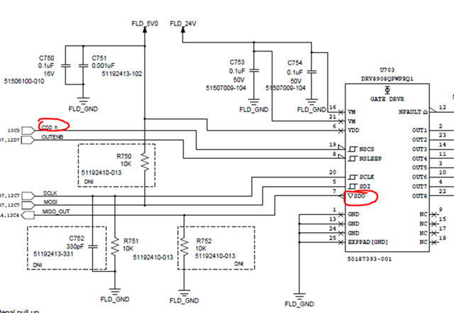
1.Would you please help to check why is the “OLD” happened when we add Direct Air Discharge: +/- 8KV noise to output shield line, thanks!   

And I have check that register about OLD configration is back to default, why? and the register(address 0x07) is not back to default value,why?

2. can you tell me If there any other cases that would re-enable the open load detection (OLD)  ;

3.  can you tell me If there any special notification about the sets of registers when disable OLD;

  • Hello,

    The DRV8908-Q1 has no system level ESD protection.  External protection for this type of testing would need to be added.  It is not reasonable or advised to test the device with a system level ESD strike with no protection.  Device could be easily damaged.

    https://www.ti.com/lit/an/slyt492/slyt492.pdf

    Regards,

    Ryan

  • hi kehr,

    thank you for your answer. this question is solved,becasue  the nSLEEP signal get impacted, and re- initial the chips,in the ESD question.

     I have another question.We use 4 piece of  drv8908_Q1 chips, and 4 chips use the same CLK, MOSI,MISO, but 4 CS  of drv8908_Q1 are  different GPIO.

    we want to initial 4 chip together to reduce initialization time,

    if we could enable 4 chips’ NSCS pin at the same time, then write 4 chips’ registers together?

    If we do like this, if the SDO pin would damaged when 1 chip’s SDO is HIGH, and another is LOW because 4 chips’ asynchronous reply? Thanks! 

  • Hello,

    This is not recommended.  Please use daisy chain feature as discussed in the datasheet in section 8.5.3.  This will also save CS pins.

    Regards,

    Ryan

  • hi  Rayn

         my schematic has decieded  use 4 CS pins, without  chain feature. 

    Now ,i want to save  intialization  time , when mcu set CS is low, can mcu  write 3 regiters in sequence?  In other words, MCU set CS low, MCU write first register and read SDO data, then write second register and read SDO data,then write  third register and read SDO data, finally set CS is high?   this method is ok?

    thanks.

  • hi  Rayn

         my schematic has decieded  use 4 CS pins, without  chain feature. 

    Now ,i want to save  intialization  time , when mcu set CS is low, can mcu  write 3 regiters in sequence?  In other words, MCU set CS low, MCU write first register and read SDO data, then write second register and read SDO data,then write  third register and read SDO data, finally set CS is high?   this method is ok?

    thanks.

  • Rita,

    Please check datasheet and read the second bullet about nSCS pin.  It must be taken back HIGH for at least 400ns.

    Regards,

    Ryan

  • hi   Ryan

      thank you again . And I have another question ,for Slew Rate Control register(address is 0x1d),  when MCU set to 0xff ,  output slew rate faster than default(when set to 0x00),right?

  • Rita,

    That is correct.

    Regards,

    Ryan