This thread has been locked.

If you have a related question, please click the "Ask a related question" button in the top right corner. The newly created question will be automatically linked to this question.

DRV8301: MCU & Driver failures at higher duty/run full SW

Part Number: DRV8301
Other Parts Discussed in Thread: TPS54260

One of my college student is having the below described issue.
Application : BLDC Motor- 12V/2A max rating with DRV8301 Driver IC.

Below are the stage wise development activities.

  • Stage 1 : Both are EVMs (DRV8301-TI, STM32- ST). Tested OK
  • Stage2 : DRV8301-redesigned inhouse + STM32-ST. Tested OK
  • Stage3 : Main Board-Designed in house (with both DRV8301, STM32). PCB Assembled by manual soldering.
    1. Individual section testing : Motor tested ok by driving through MCU. LCD also tested OK.
    2. While running all together
      1. MCU Burnt in 1 board.
      2. Motor driver IC DRV8301 burnt in 1 board.
  • Motor drive is OK at 60% without display. When we connect the LCD connector at that speed, the driver IC/MCU damages. Arcing is observed on driver IC. 3V3 short to GND. Removed all 3V3 ICs, still there was a short.

    As i mentioned, its a college project. they dont have proper set up & tools to capture the data and send.
    If TI helps by telling possible causes for this issue, i will try to help them to sort it out. 
     LCD_Display_AutoCPAP schematic.pdf
  • Hi Reddy,

    I will need some time to look into this, I will get back with you next week.

    Best Regards,

    Joshua

  • Hi Joshua,
    Kindly update on this

  • Hi Reddy,

    I would recommend checking that the current being pulled from the DVDD pin is not exceeding 1.5 A and what voltage value is being output from the DVDD pin.

    Best Regards,

    Joshua

  • I checked the layout.

    1) observed PVDD1 cap is 0.1uF on board. Placed on other side of the driver IC  (but recomomnded 4.7uF, Close to driver)

    2) observed PVDD2 cap is  2.2uF on board. Placed on other side of the driver IC at 50mm distance  (but recomomnded 4.7uF, Close to driver)

    i think this can create trouble on the board right

  • Hi Reddy,


    You are correct, distance between the PVDD pin and their respective capacitors can affect the capacitors ability to protect the device from high frequency noise and supply large currents for when the motor driver switches.

    Looking at the schematic you provided the capacitors for the PVDD pins seems to be the correct values. Although there should be a bulk capacitor, we recommend using a 4.7 uF capacitor, along with the 0.1uF capacitor for PVDD1.


    I would recommend reading the Best Practices for Board Layout of Motor Drivers app note (LINK) for more information.


    Could you tell me the purpose of the LCD screen in the system, does it interact with the motor driver?


    Thank you,

    Joshua

  • What is the recommonded buck inducatance & Output capacitance value if input voltage is 24V (PVDD2) & Output is 3V3,1A. 
    Is it mandatory to keep charge pump cap value as 0.022uF ?? If yes Why ?? Can i use 0.1uF. 
    Do we need to have sepearte GND planes of MCU, driver & Join as star. 

  • Hi Reddy,


    In general we recommend using a 22uH inductor and 4.7uF capacitor for 3.3v output, but I would recommend using the Webench tool (LINK) we have for finding optimized component values for your needs, the buck in the DRV8301 is the same as the TPS54260.


    You do not need to have separate ground planes, just make sure that the path of the digital signals and the analog signals on the ground plane will have minimal crossover to prevent excessive noise on the digital signals.


    I will have to reach out to colleagues about the charge pump cap value and will get back to you on this in a few days.

    Thank you,

    Joshua 

  • Hello Reddy,

    We would not recommend changing the charge pump capacitor from 0.022uF to 0.1uF. 

    Changing the charge pump capacitors value will change the average current on the GVDD pin and the current capacity of the charge pump regulator.  The DRV8301 was characterized with the a charge pump capacitor value of 0.022uF so we cannot guarantee the value of the current on GVDD if the capacitor is changed.  

    Best Regards,

    Joshua

  • I prepared one board as per TI Datasheet recommonded values and tried to test basic sections like 3V3 & Gate waveforms.
    While testing 3V3 output i obsorved up to 300mV with just <200mA load. This is not a big concern.
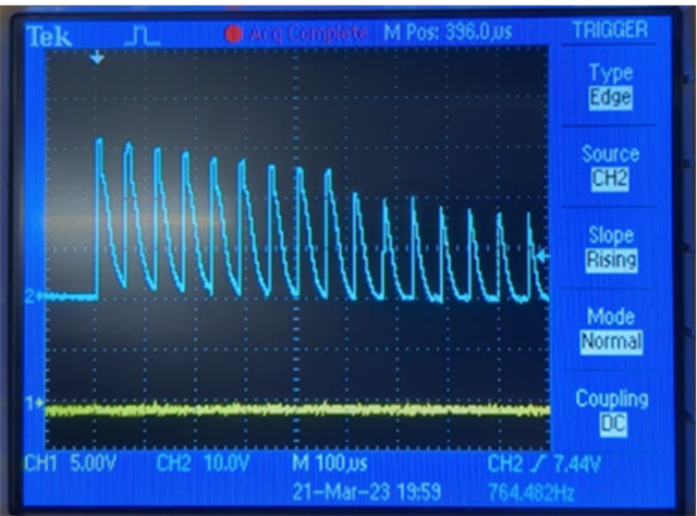
    1) While testing one leg of the H-Bridge (without motor connected) i obsorved High side gate pulse to be different than expected. Kindly review the waveforms below. CH1= Leg-A Low side Fet Q6Vgs, CH2= Leg-A High side Fet Q3 Vgs. Gate rise time of both Low side & High side FETs are <0.2uS which is perfect.
    2)  Current sense amplifier pins (SN1, SP1)  if un used , do i need to leave those floating or connect to GND.

  • Hi Reddy,

    1. Was this condition occurring when the device was in the motor spinning mode, motor breaking mode, or was it on startup?

    2. Could you send me captures of the INHx, INLx, GHx, and GLx pins as well?

    2)  Current sense amplifier pins (SN1, SP1)  if un used , do i need to leave those floating or connect to GND.

    Tie SN1 and SP1 together and connect to ground, leave the SO1 pin floating.

    For more information on handling unused CSA pins please see section 6. Unused CSA of the following FAQ: [FAQ] Quick Guide to Debugging Common Issues in BLDC motor drivers.

    Thank you,

    Joshua

  • Hi Reddy, 

    Please let us know if further assistance is needed - or if Joshua's latest comments helped you resolve your debug. 

    Best Regards,
    Andrew