This thread has been locked.

If you have a related question, please click the "Ask a related question" button in the top right corner. The newly created question will be automatically linked to this question.

DRV8301: Unexplained high side gate driver failure.

Part Number: DRV8301
Other Parts Discussed in Thread: DRV8323

I've had an ebike system running flawlessly, with a sensorless, Instaspin, FOC, C2000 device + DRV8301, for the last five years. All of a sudden the system fails with the fault isolated down to the DRV8301. Upon inspection it appeared as if a small fleck of solder, or similar, could have landed across two pins and shorted them together, causing the failure. The DRV8301 was replaced, in situ, and the system sprang back to life. It then failed again a couple of days later.

Obviously the first failure wasn't caused by a fleck of solder.

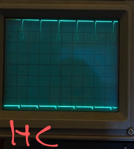
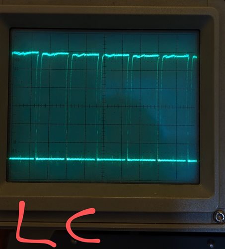
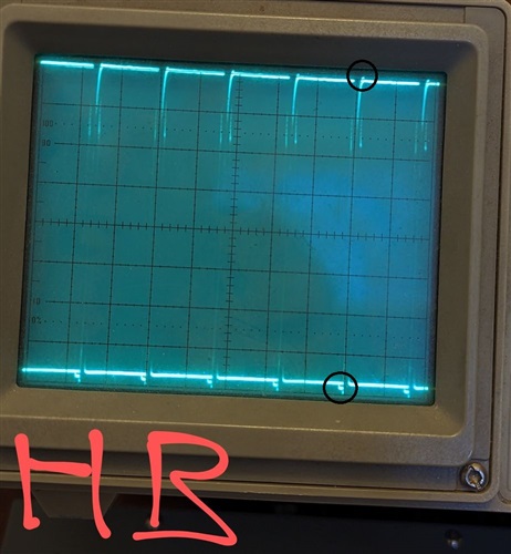
The faults have been isolated to the high side gate drivers and are relatively minor as faults on these forums go. First time SH_C and GH_C ended up shorted internally @ about 4 ohms internal resistance. Second time SH_B and BST_B ended up shorted together at about 20 ohms. Interestingly neither of these conditions were enough to affect the charge pump to the degree that the system stops working and a fault flags. The associated high side stops but the system still gives it's best shot at spinning the motor. It works but at significantly lower power output and the harmonic content shoots up (away from sinusoidal drive) so the acoustic noise increases.

Having gone five years with reliable operation I do not think that layout, component choices, or system tuning is to blame. More component values/performance drift/component failure over time could be the most likely culprit. Sadly I do not have the PCB layout anymore but given how reliable it's been, up until now, I do not think that's to blame. The gate drivers are configured for their lowest peak current delivery and 10 ohm gate resistors are used. The MOSFETs have a total gate charge of 89nC and the system is set to run at 30kHz (well within the DRV8301s capabilities). A TVS is installed across the supply along with 1000uF of bulk, low ESR, capacitance. The supply is a high current lithium ion battery pack so sinking back EMF shouldn't be a problem. The TVS hasn't been positioned specifically to protect the DRV8301 and the battery is a considerable distance away, as parasitics go, so that's not completely ruled out.

System nominal is 48V and the system drives up to a limit of 18A as set in the Instaspin software.

I obviously realise that this is a bit of a needle in a haystack, but given the way in which the high side gate drivers have failed, is this failure, after years of use, indicative of anything in particular I can focus on in terms of solving this problem?

Clearly something has changed within the system but I would rather isolate, and diagnose the issue, instead of replacing all the power components and hoping that fixes it. Scoping the gate drive signals would be the first thing I'd want to do but I figured I would ask here first before I go poking around as that always comes with the potential for causing further damage. 

Many thanks,

Matt.

  • Hi Matt,

    Thank you for posting your question to the motor driver forum! I will look into your question in more detail and aim to get back to you by the end of the week.

    Regards,

    Anthony Lodi

  • Hi Matt,

    Given that the damage is occurring on the device outputs I would look at the GHx, SHx, and BSTx waveforms and look to see if there are any voltages that are operating close to the abs max ratings of the device. I would recommend doing this on an undamaged board as well as on the damaged board. I am particularly interested in the waveforms during peak current, since the effects of parasitics are worse during that time. One consideration is that the device has an abs max of 65V, so with a 48V rail you have a low margin for spikes or supply pumping. Generally we recommend 100V devices for 48V supplies to provide better margin.

    Regards,

    Anthony Lodi

  • I've had an ebike system running flawlessly, with a sensorless, Instaspin, FOC, C2000 device + DRV8301, for the last five years. All of a sudden the system fails with the fault isolated down to the DRV8301. Upon inspection it appeared as if a small fleck of solder, or similar, could have landed across two pins and shorted them together, causing the failure. The DRV8301 was replaced, in situ, and the system sprang back to life. It then failed again a couple of days later.

    Obviously the first failure wasn't caused by a fleck of solder.

    Hi Matt,

    So what do you think the source of the solder flake? Did you find any damage to the power FETs?

    It's rated at 65v ABS, so 48v batt is a good margin. I don't blame the driver but would looking at the FET timing and thermal issue. I think a damaged FET leading to leakage voltage/current to damage the driver.

    Brian

  • Yes ideally I'd be using one of the newer parts, that has a higher abs max, for a greater margin of safety but when this system was built these were not on the market. I don't even think the first smart drivers, the DRV8323 series, were out then either.

    It is possible, that when first constructed, any parasitics were well controlled by the surrounding components. Then as time has gone on things have begun to slip. The only part that would really be affected by this is the bulk electrolytic unless a ceramic one had failed. In my experience these usually fail short circuit and then, potentially, explode (so are obvious) although given the application is subjected to significant vibration it's possible a decoupling capacitor may have cracked at one of its terminals.

  • The flake of solder could have been accidentally introduced during a period of maintenance when another part of the ebikes electronic systems were modified  - they share a common enclosure. I don't think the fleck actually did anything but you never know.

    Damage to one of the FETs was my first thought, as I've seen partially damaged FETs take out drivers in the past, but would you expect a damaged FET, in phase C, to destroy the high side driver in phase B? That would seem bizarre although maybe more than one FET has developed a fault.

    It's worth pointing out that both failures occurred at either motor start-up or when the motor was commanded to stop, not when the motor was spinning. Motor start-up has always been extremely smooth, and, without any kind of jerkiness that could cause big current demands on the bus. During start-up, and when the motor is running, the FETs are always engaged too. However, when commanded to stop, the FETs are transitioned to high-Z and any back EMF generated, during the coasted deacceleration and sudden disengagement, then has to be dealt with by the MOSFET body diodes onto the supply bus. Given the battery, and TVS, that shouldn't be a problem but wouldn't this also be the time when the SH_X node could be driven negatively? Again I'd have expected the body diodes, in the low side FETs, to start conducting if the SH_X node went below ground but I suppose the current shunts, in series with the FETs, could raise this voltage to something unacceptable for the driver to withstand and then the diodes might also not be fast enough. 

    This also brings up the question of why now? I definitely need to get in there with the scope and see what's going on.

  • The only part that would really be affected by this is the bulk electrolytic unless a ceramic one had failed.

    Bulk cap failed cannot damage the driver or FETs, but it can cause noise that affects the function of the driver.

    It's worth pointing out that both failures occurred at either motor start-up or when the motor was commanded to stop, not when the motor was spinning. Motor start-up has always been extremely smooth, and, without any kind of jerkiness that could cause big current demands on the bus

    Which method do you use to align the rotor initial position for this sensorless driver -- IPD or Align? Since the ebike always has load so I would think you use IPD. 

    I don't think it's matter which output channel is damaged, it can affect the input behavior. 

    Brian

  • Hi Matt,

    Thanks for the additional background, that makes sense. I think that the best next steps would be to look at the  GHx, SHx, and BSTx waveforms to see if there could be some operation close to abs max especially during startup and braking. Startup will generally result in higher current draw which could result in greater ringing during that time. Hi-Z braking will also cause high currents flowing through the body diodes of the FETs and could cause some negative and positive transients especially on SHx during that time.

    Regards,

    Anthony Lodi

  • I considered that if the bulk cap had increased ESR and reduced capacity, due to aging, that the bulk caps ability to help suppress transients could potentially lead to increased stresses placed on the driver but I think this is unlikely.

    The controller is using Instaspin FOC, with the FAST estimator, integrated into a TMS52F package. As far as I am aware this is using something like IPD, with high frequency injection, to detect the rotor position at low levels of BEMF, and then starts up with the control loop closed.

    In this case the motor isn't always connected to the spinning wheels as it's a mid-drive configuration that drives the front chain ring. When you stop pedalling, the motor disengages and then stops completely as the bike freewheels along. It doesn't windmill except for the instance when you stop and start the motor very quickly but this doesn't happen that frequently.

  • So I got in there, with the broken driver chip, to start scoping and everything looked fairly good. The broken phase was a considerable mess and it impacted the drivers ability to control the drive signals to the other phases so anything detailed was impossible. I thus replaced the DRV8301 and went from there.

    Starting off I disconnected the motor as that would only complicate things. Straight off the bat phases A and C looked perfect but B still looked a mess. This was not expected. After some investigating it turned out that phase Bs low side MOSFET, SMD package, source, solder points weren't connecting to ground properly and the bootstrap capacitor wasn't getting to charge. I can only speculate that the thermal cycling, over 5 years, of the power stage had gradually caused the solder points to fail and with the replacement DRV8301, a couple of weeks ago, completely breaking what little contact there was left. Now this would definitely cause problems as any negatively going inductive spike, during High-Z braking, would then not be able to conduct through the body diode and out would go the magic smoke.

    This also make senses as a failure mode that would only occur after an extended period of use. Hopefully this will be the fix that was needed. I'll get back here with some scope shots later as I ran out of time before after fixing the hardware.

  • Hi Matt,

    Great to hear that it looks like you found the root cause! Your analysis makes sense. Let me know if you have any additional issues after fixing the phase B low side MOSFET. 

    Regards,

    Anthony Lodi

  • I think a damaged FET leading to leakage voltage/current to damage the driver.
    After some investigating it turned out that phase Bs low side MOSFET, SMD package, source, solder points weren't connecting to ground properly and the bootstrap capacitor wasn't getting to charge. I can only speculate that the thermal cycling, over 5 years, of the power stage had gradually caused the solder points to fail and with the replacement DRV8301, a couple of weeks ago, completely breaking what little contact there was left. Now this would definitely cause problems as any negatively going inductive spike, during High-Z braking, would then not be able to conduct through the body diode and out would go the magic smoke.

    I was guessing the bad FETs led to damaged driver, but a bad Source connection can do the same. I don't think the FET was hot enough to cause the bad solder joint at the Source -- if Drain is the hottest terminal and if the FET was hot enough to melt the solder then it's already in trouble. I would investigate the pcb assembly process with the bad solder joints. Yes, with the low side FET with high impedance, whenever the high FET turned off during PWM cycle, there was a very high voltage spike at driver HSx pin and can damage it. 

    In this case the motor isn't always connected to the spinning wheels as it's a mid-drive configuration that drives the front chain ring. When you stop pedalling, the motor disengages and then stops completely as the bike freewheels along.

    I thought the motor is in the wheel hub and always connected. How is the motor disconnected from the wheel -- via mechanical gear linkage or electro-magnetic clutch? So most of the time when starting from complete stop the motor is disconnected from the load then I would think using the Align (rotor to the energized stator coils) is a better way than IPD.

    Brian

  • Oh no I'm not saying that the FET was hot enough to melt solder. Thermal cycling, with SMD soldering, is a well known cause of solder point failure, especially in BGAs. I can only assume a similar thing happened here. 

    Imagine cycling a normal bike. When you pedal forwards the chain engages the sprocket on the rear wheel and you turn the rear wheel forwards. If you stop pedalling the sprocket on the rear wheel disengages via the freewheeling system and you hear the typical clicking noise. This prevents the pedals from being turned forwards if you stop pedalling. With a mid drive motor system the motor turns the front chain ring that's attached to the pedals. In this way the freewheeling system on the rear wheel means the motor is automatically disengaged from the wheels when it's spinning slower than the bike is moving forwards. When starting off from a stand-still the motor is always engaged so you need the FAST estimator. If the motor is turned on with the bike moving then it has to speed up to match the speed of the bike before it engages with the rear wheels.

    Anyway here are some gate driver images from the working system. 

    Given the nature of the system it was impossible to get in there with the probe directly and use a coil spring around the tip of the probe to ground. Thus the measurements include some noise and small high frequency inaccuracy from the flying leads that were soldered to the PCB. This is with the system driving the motor with each minor division = 1V.

    Anyway to my eyes things look okay. With a little peaking (1-2V) on the high sides during the dead time hand off to the low sides. This is one area I would expect to improve with one of the newer smart drivers as it would automatically tune the dead time down to a minimum but let me know what you think.

  • Hi Matt, 

    Waveforms look pretty good. Could you annotate on the waveforms what you are referring to when you mention the 1-2V peaking on the high sides? 

    Regards, 

    Anthony

  • Thanks Anthony and sure here you go.

    Inside the black circles are slight changes in the gate drive signal around the transition from high-side to low-side. Maybe this is normal during the hand-over and deadtime. Certainly it looks very well damped if it is ringing of any kind.

  • Hi Matt, 

    This could be related to body diode conduction, in which case reducing deadtime would only reduce the duration, not necessarily the magnitude of the voltage. I think the positive spikes at the top of the waveform are likely overshoot, but am not positive. Are there 2 signals displayed on the screen? it is showing the signal both high and low at the same time, so I am wondering if this is 2 signals overlaid. 

    Regards,

    Anthony Lodi

  • This is with the system driving the motor with each minor division = 1V.

    If the gate signals have 1v/div, then the GLx is only 6v and GHx is 8v, which is not normal. Also the scope pics look strange: both the high level and ground level of the pwm signal have the same about 80% duty cycle instead of 80% high then 20% ground. I'm not sure what I am looking at.

    Brian

  • Yes for some reason it's the way this analogue scope is triggering off the signal is quite annoying.

  • It's not 1V per major division. It's 1V per minor division on the high side, so 5V per major. It's swinging almost 40V on the high side gate.

    The low side is 2V per major division, so almost 12V swing on the gates.

    This scope doesn't have advanced triggering functions, from what I can see, to correctly display the waveforms. That's why things look the way they do.

    A bit like when a scope can accurately trigger on steady clock signals but if you try and trigger on a data line all you see is an overlapping up and down mess. That's what is happening here as the control loop spins the motor.

  • Hi Matt,

    That makes sense about the triggering of the waveforms. My analysis is that the -2V comes from the conduction of the body diode of the FET, which is more of a MOSFET parameter and not so much related to the driver. A newer driver may allow for shorter deadtime, but the magnitude of the voltage drop across the body diode will be determined by the FET characteristics. No concern from my end on the waveforms (as best as I can tell with the limitations of the scope).

    Regards,

    Anthony Lodi

  • Thanks Anthony and that's taught me something about what reverse recovery looks like on a scope too.

    Let's just hope it remains reliable! I am drawing up a design around one of the higher voltage smart drivers just in case.

  • Sounds good!

    Regards,

    Anthony Lodi