This thread has been locked.

If you have a related question, please click the "Ask a related question" button in the top right corner. The newly created question will be automatically linked to this question.

DRV8106-Q1: DRV8106-Q1 Register can only be read once by SPI second read send 0x00 value

Part Number: DRV8106-Q1

Ive the same behavior for all register, first read aftec POR send back default value written into datasheet, second read give 0x00.

This is true when ever I read all register once, then redo reading loop, or reading  a single register twice.

Changing register value, even IC_CTL to remove lock field is not working.

~~~~~~~ Info about test made ~~~~~~

Test sequence :

Set SLEEP and DRVOFF pin to wakeup the driver

Assert CS pin

Shift address + read flag and a dummy value

Get status and register value

Result for DRV_CTRL_1

First read :  Status = 0xC0 Value = 0XFF

Second read Status  = 0xC0 Value = 0x00

Note:

  • Reading IC_STAT_1 send back 0x40 value : POR set and SPI NOK
  • When I  insert a toggle of SLEEP and DRVOFF pin  before second read , the second read works ( but DRV8106 had be reset in between as forcer to for to sleep mode)

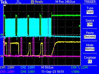
Below SPI capture ( MOSI in pink, MISO in yellow ) : 1 sucessfull read ( status 0xC0 data 0xFF), then 2 failled  read 0xC0 status and 0x00 data  

  • Issue affection only register above IC_CTL register ($0x04), readonly registers can be read multiple times without issue

    When a R/W register is read twitch ( and second read send 0x00, other registers can still be read with success. Il look like a kink of softlock.

    13:44:06.110 -> ===Reading===
    
    13:44:06.110 -> IC_STAT_1  Received: C0-40
    
    13:44:06.110 -> VGS_VDS_STAT  Received: C0-0
    
    13:44:06.110 -> IC_STAT_2  Received: C0-2
    
    13:44:06.110 -> IC_CTRL  Received: C0-6
    
    13:44:06.110 -> BRG_CTRL  Received: C0-0
    
    13:44:06.110 -> DRV_CTRL_1  Received: C0-FF
    
    13:44:06.110 -> DRV_CTRL_2  Received: C0-FF
    
    13:44:06.110 -> DRV_CTRL_3  Received: C0-20
    
    13:44:06.110 -> VDWS_CTRL1_  Received: C0-20
    
    13:44:06.110 -> VDS_CTRL_2  Received: C0-DD
    
    13:44:06.110 -> OLSC_CTRL  Received: C0-0
    
    13:44:06.110 -> UVOV_CTRL  Received: C0-14
    
    13:44:06.110 -> CSA_CTRL  Received: C0-1
    
    13:44:06.110 -> ===Writting===
    
    13:44:06.110 -> ===Reading===
    
    13:44:06.110 -> IC_STAT_1  Received: C0-40
    
    13:44:06.110 -> VGS_VDS_STAT  Received: C0-0
    
    13:44:06.110 -> IC_STAT_2  Received: C0-2
    
    13:44:06.110 -> IC_CTRL  Received: C0-6
    
    13:44:06.110 -> BRG_CTRL  Received: C0-0
    
    13:44:06.110 -> DRV_CTRL_1  Received: C0-0
    
    13:44:06.110 -> DRV_CTRL_2  Received: C0-0
    
    13:44:06.110 -> DRV_CTRL_3  Received: C0-0
    
    13:44:06.110 -> VDWS_CTRL1_  Received: C0-0
    
    13:44:06.110 -> VDS_CTRL_2  Received: C0-0
    
    13:44:06.110 -> OLSC_CTRL  Received: C0-0
    
    13:44:06.110 -> UVOV_CTRL  Received: C0-0
    
    13:44:06.110 -> CSA_CTRL  Received: C0-0
  • SPI R/W sequence ( arduino had been used to controls our mockup board

    //============================================================================//
    // NAME: vTI_SPIRWRegister  
    //============================================================================//
    // ROLE: RW register from a single DRV8106S device
    //----------------------------------------------------------------------------//
    // REQ:
    //----------------------------------------------------------------------------//
    // INPUT:
    // u8Write : 1 write / 0 Read
    // u8Address reg address
    // u8DataIn : data to write
    // pu8StatusOut : pointer on status reading
    // pu8DataOut : pointer on data reading
    // OUTPUT: status and read data (2 byes)
    //============================================================================//
    void vTI_SPIRWRegister(uint8_t u8Write, uint8_t u8Address, uint8_t u8DataIn, uint8_t *pu8StatusOut ,uint8_t *pu8DataOut  )
    {
      uint16_t u16RxTxBuf = 0U;


      //Assert CS
      digitalWrite(TI_CS_PIN, LOW);

      //Prepare command buffer bits order  b7 to b0
      //first byte  : 00 W0 A5 A4 A3 A2 A1 A0
      //second byte   D7 D6 D5 D4 D3 D2 D1 D0
      //For a write command (W0 = 0), the response word consists of the fault status indication bits
      //followed by 8 null bits.
      //For a read command (W0 = 1), the response word consists of the fault status indications bits
      //followed by the data currently in the register being read.
      u16RxTxBuf = (uint16_t)((u8Address & 0x3FU))<<8U+ (uint16_t)(u8DataIn);

      if(u8Write != 0U) //Add flag if write needed
      {
        u16RxTxBuf |= 0x4000U; //Set bit 14
      }

      u16RxTxBuf=  SPI.transfer16(u16RxTxBuf);

      //Deassert CS
      digitalWrite(TI_CS_PIN, HIGH);

      //Get status from Rx buffer
      *pu8StatusOut = (uint8_t)(u16RxTxBuf>>8)&0xFF;

      //Get data from Rx buffer  
      *pu8DataOut = (uint8_t)(u16RxTxBuf&0xFF);

      return;
    }
  • Test sequence using EVB firmware value, DRV_CTL cannot be changed to EE

    Answer to write command is supposed to send back 0x00 data, get supect 0x40 value

    15:18:46.672 -> DRV8206 test V0.1
    
    15:18:47.674 -> ===Writting===
    
    15:18:47.674 -> Send IC_CTL: 87 Received: C0-40
    
    15:18:47.674 -> Send BRG_CTRL: 0 Received: C0-0
    
    15:18:47.674 -> Send DRV_CTRL_1: EE Received: C0-40
    
    15:18:47.674 -> Send DRV_CTRL_2: EE Received: C0-40
    
    15:18:47.674 -> ===Reading===
    
    15:18:47.674 -> IC_STAT_1  Received: C0-40
    
    15:18:47.674 -> VGS_VDS_STAT  Received: C0-0
    
    15:18:47.674 -> IC_STAT_2  Received: C0-2
    
    15:18:47.674 -> IC_CTRL  Received: C0-6
    
    15:18:47.674 -> BRG_CTRL  Received: C0-0
    
    15:18:47.674 -> DRV_CTRL_1  Received: C0-FF
    
    15:18:47.674 -> DRV_CTRL_2  Received: C0-FF
    
    15:18:47.674 -> DRV_CTRL_3  Received: C0-20
    
    15:18:47.674 -> VDWS_CTRL1_  Received: C0-20
    
    15:18:47.674 -> VDS_CTRL_2  Received: C0-DD
    
    15:18:47.674 -> OLSC_CTRL  Received: C0-0
    
    15:18:47.674 -> UVOV_CTRL  Received: C0-14
    
    15:18:47.674 -> CSA_CTRL  Received: C0-1
  • Switching OFF PVDD, UV condition is detected as expected, but writing IC_CTL to clear fault get not effect

    16:02:53.756 -> Send IC_CTL: 87 Received: E4-64
    
    16:02:58.763 -> ===Reading===
    
    16:02:58.763 -> IC_STAT_1  Received: E4-64
    
    16:02:58.763 -> VGS_VDS_STAT  Received: E4-0
    
    16:02:58.763 -> IC_STAT_2  Received: E4-82
  • SPI_OK bit is now set, fixed by setting up SCK, and other control signal to relevant state prior de-asserting SLEEP signal.

    How ever write doesn't work, and read for resiter 0x05 to 0x0D work only once ( read as zeros after first read)

    Write flag correctly set  IC_CTL read 0x0400  is sent over SPI , write 0x4400 is sent over SPI

    UV reporting works , but cannot be cleared due to register write issue

  • Hey Jerome,

    I've pinged our Automotive expert to get his thoughts on this.

    Do you have a DRV8106S-Q1EVM with you that you can test and compare with? You could use a logic analyzer or scope to compare your SPI commands to the EVM's.  

    And have you double checked that your SPI timing and CS/CLK polarity and edge setup match 6.6 Timing Requirements? Just want to cover the basics first.  

    Regards,

    Jacob

  • Hi,

    As Jacob pointed out, better to check 6.6 Timing requirements. And EVM and logic analyzer could help.

    If you are seeing SPI_OK, MCU may send more or less than 16CLK while nSCS is low.  Here is example for DRV family device with successful communication.  B15 and B14 should be 11 and SCLK should be just 16clk. Better to check those as Jacob mentioned.

    And nSLEEP should be high and DVDD should be good stable supply for SPI communication. 1uF cap is recommended between DVDD pin to GND.

    regards

    Shinya Morita

  • I've found the issue, R/W bit logic  was inverted.

    Thanks