This thread has been locked.

If you have a related question, please click the "Ask a related question" button in the top right corner. The newly created question will be automatically linked to this question.

DRV8231: Application questions

Part Number: DRV8231


Tool/software:

Hello TI team

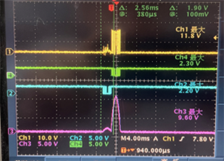
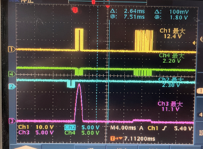
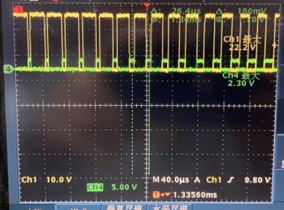
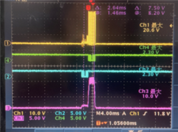
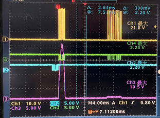
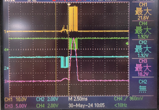
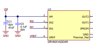
There is a Haptic application with loading(Coil 6.8 ohms),Input Voltage is 21.4V, Vref is 5V, and ISEN connected to GND.
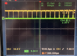
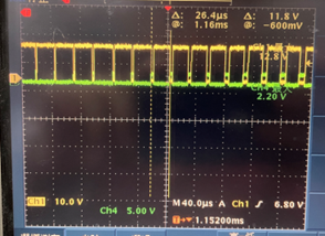
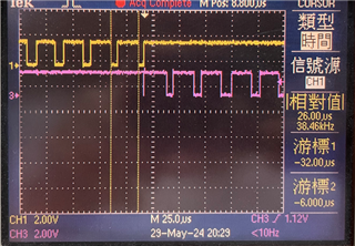
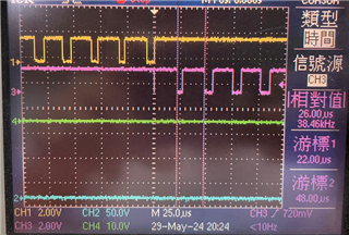
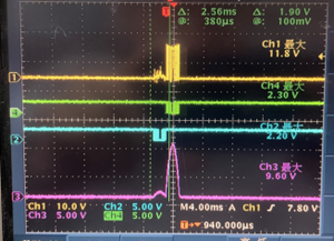
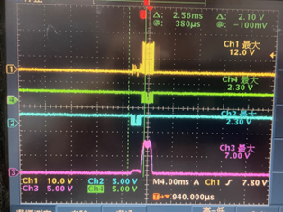
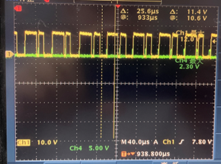
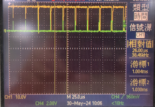
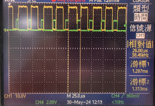
The experiment found that when the input voltage is 21.4V, the Voltage duty cycle of the OUT PIN and IN PIN (PWM) is different from that when the  input voltage is 12V. In addition to other experiments, when there is no loading and the  input voltage is 21.4V or 12V, the Voltage duty cycle of the OUT PIN and IN PIN (PWM) are the same, as shown in the figure.
I want to understand why the  input voltage is 21.4V, Vref is 5V, ISEN connected to GND(it seems to meet the specifications of Drv8231),but the Voltage duty cycle is different?  Is there any part that has not been noticed?
Will there be any problem with the above conditions (The loading(coil 6.8 ohms), Input Voltage is 21.4V, Vref is 5V, and ISEN connected to GND) with Drv8231? Thank you!! 

  • Hello TI team

    Supplement:

    1. Logic input Voltage Level is 1.8V.

    2. Since the system cannot successfully upload the measurement waveform, if it is necessary to provide waveform confirmation, is there any other way to provide the waveform to your company for confirmation?

  • Hi Daven,

    A picture of the waveforms would be helpful, I am not sure what you mean by "different waveforms". If possible, I would suggest copy and pasting a screen shot of the waveforms into the text box. 

    When you say "input voltage" do you mean, VM is 21.4V and 12V?

    What duty cycle and frequency are your input signals (IN1 & IN2)?

    Best,

    David

  • Hi David

    The waveform is as follows: (CH1: OUT-; CH2: INT1; CH3: OUT- after Low PASS Filter; CH4: INT2)  
    1. VM:12V, Loading: Output Connected Coil (6.8ohm) ,Verf:5V, ISEN connected to GND


    2. VM:21.4V, Loading:Output  Connected Coil (6.8ohm) ,Verf:5V, ISEN connected to GND


    3. VM:12V, Loading: Output  no Connected Coil ,Verf:5V, ISEN connected to GND


    3. VM:21.4V, Loading: Output  no Connected Coil ,Verf:5V, ISEN connected to GND


    4. the input signals (IN1 & IN2) frequency  is 38.46KHz.(CH1: INT1; CH3: INT2)

    Thanks!!!!

  • Hi Daven,

    Please allow me some time to review these waveforms. I will get back to you later today or tomorrow.

    Best,

    David

  • Hi David

    I have sorted out some questions as follows:

    1. Why are their Output (before & after Low PASS filter) waveforms different between Loading: Output Connected Coil (6.8ohm) and Loading: Output  no Connected Coil? Does the IC have any activation mechanism?

    • VM:21.4V, Loading:Output  Connected Coil (6.8ohm) ,Verf:5V, ISEN connected to GND


    • VM:21.4V, Loading: Output  no Connected Coil ,Verf:5V, ISEN connected to GND


    2. VM:12V, Loading:Output  Connected Coil (6.8ohm), ISEN connected to GND, when Vref is 5V or 3.3V, does the IC not limit the Output  current? Why does the OUTPUT waveform (before & after Low PASS filter) will be different when Vref 5V or 3.3V?

    • Verf:5V

          
    • Verf:3.3V


    3. Continuation of question 2, VM:12V, Loading:Output  Connected Coil (6.8ohm), ISEN connected to GND, Vref is 5V. Why does the Output  waveform (after Low PASS filter) change when VM:12 increases to 21.4V ? Does the IC activate any mechanism?

    • VM:12V

           
    • VM:21.4V


    4. Continuing from question 3, why does the Loading change (Output  Connected Coil 6.8 to 12.2ohm), VM: 21.4V, Vref: 5V, Output  waveform (after Low PASS filter) improve? But not when Vref: 3.3.

    • VM:21.4V,Loading:Output  Connected Coil (12.2ohm),Vref :5V


    • VM:21.4V,Loading:Output  Connected Coil (12.2ohm),Vref :3.3V


    Thanks~~~

  • Hi Daven,

    I am a bit confused on what the two output waveforms are with one "before" and one "after" low pass filter. 

    Are you implementing an external low pass filter on the board?

    Could you please elaborate or include a circuit diagram and layout to better understand?

    Best,

    David

  • Hi David 

    The Low pass filter is just for the convenience of observing the difference in the H-Bridge output signal under different conditions (such as VM, Vref, ISEN). The Low pass filter will not be added to the actual circuit.

    The design requirements are VDD-H: 21.4V (Maximum voltage provided by the motherboard) and the coil resistance needs to be matched with 8.24ohm. The picture below shows the circuit, VDD-H =: VM, Vref =5V or 3.3V; ISEN connected to GND, OUTP & OUTN solder points will be connected to Coil.Have questions about the requirements or circuit design part?

    The layout part hasn’t started yet.  Thanks!!! 

  • Hi Daven,

    If possible, I would try connecting VREF to GND instead of DGND. The DRV8231EVM connects all input signals to GND reference. 

    The full schematic is available in the hardware files of the DRV8251EVM Evaluation board | TI.com product page. 

    Best,

    David

  • Hi David

    I'd like to know what is the purpose of connecting Vref to GND?  And the Output signal waveforms under different VM voltage & Loading resistance & Vref voltage conditions were previously provided. Under some conditions, the Output signal has a voltage drop. What may cause the Output signal to drop?
    Thanks!!!
     
  • Hi Daven,

    The output signal drop could be from not enough bulk capacitance. I would suggest increasing the bulk capacitance and the rated voltage they are rated for. 

    Example from EVM schematic. 

    Best,

    David