This thread has been locked.

If you have a related question, please click the "Ask a related question" button in the top right corner. The newly created question will be automatically linked to this question.

DRV8301 low side not switching & SPI issues

Other Parts Discussed in Thread: DRV8301

Hello,

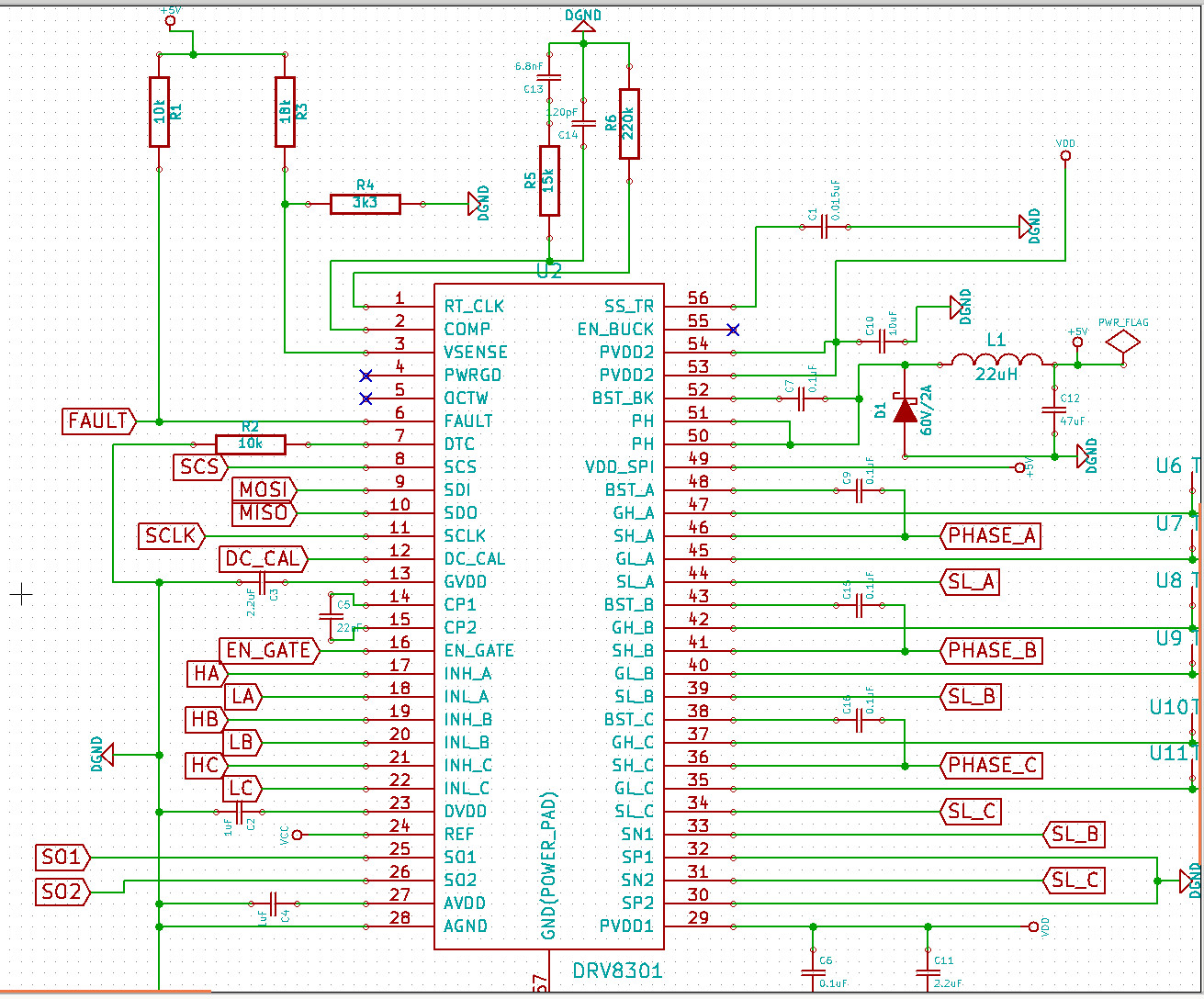
I made a custom board with the DRV8301 based on the resources and recommendations. When the board was designed, we decided to connect all the required pins so we could make the decision later in software.

Now that we've got things powered up and we think we got SPI working, there are some issues. Most of these seem related to SPI.

1. When it's all started up, we do an SPI read, which according to the docs starts with a fault condition. This indeed happens, but it also indicates a GVDD_UV condition. So the output of the first read is: 0b1000011000000000

2. The first read returns data, but other read operations always return 0. According to the data sheet, we should be able to read the contents of the control registers too, but have not been able to yet. When we use invalid frames (16-bit), the returned frames appear ok, because they indicate frame fault bits set to 1. The second status register however never returns any bit set for the device ID, even if we repeat the read multiple times. After setting the control registers and reading them back, we don't get the set values either.

3. We want to use 3-pwm mode, but this hasn't worked yet as the lower side doesn't get driven. If the lower pwm's are not left floating on the drv8301 chip, could this cause issues? The pins are not configured on the MCU.

There's another post that seems to come close to what we experience:

http://e2e.ti.com/support/applications/motor_drivers/f/38/t/365621.aspx

Here are our measurements:

  • GVDD: 11 V
  • DVDD: 3,3 V
  • AVDD: 6,5 V
  • BST_A: 10.4 V
  • BST_B: 10.4 V
  • BST_C: 10.4 V

The higher fets are switching.

Our SPI communication code looks like this (for each register setting we attempt), with the read command waiting for the RXNE to be set prior to taking the contents of the register.

uint16_t spi_transfer( uint16_t cmd )
{
    uint16_t temp;

    gpio_clear(GPIOA, GPIO15);
    // start reading control register
    spi_write( SPI1, cmd );
    while (!(SPI_SR(SPI1) & SPI_SR_TXE));
    while((SPI_SR( SPI1 ) & SPI_SR_BSY) != 0);
    temp = spi_read( SPI1 );
    gpio_set(GPIOA, GPIO15);
    return temp;
}

So we pull SCS low, then do the write, wait for TXE to complete, do a read after RXNE is set, set SCS=1 and return the result. Is this the right way to do it, or should we not set the SCS each time? According to the data sheet, the latching occurs after either the 16-th clock cycle or the SCS bit set to 1.

  • Hi Gerard

    Just a quick check before we look deep into the issue.

    Have you applied EN_GATE HIGH and VDD_SPI before you do the SPI read and write?

    Could you provide the schematic of DRV8301?

    Best regards,

  • Hi Wilson,

    The connection diagram is here:

    Everything below the line just connects to GND. C1=50V, C7/9/15/16 = 100V, C10=25V, C5=100V, C3=50V, C2/C4=25V, C14/13=50V.

    Some modifications have taken place after the board was produced:

    1. The +5V VDD_SPI was reconnected to +3.3V through a wire jumper, as the VCC for MCU is 3.3v.

    2. R1 was removed, so the FAULT indicator is not currently used by the MCU.

    We drive the VDD_SPI directly from the regulator now (3.3v), which is very low drop and was measured at 3.2v. The EN_GATE was indeed set HIGH, but our oscilloscope showed something strange there. See below.

    Here are the diagrams of the commands that we send out. There are two commands that write data (0x02|0x28) and (0x03|0x08) to achieve 3-pwm mode, only reporting oc conditions and 40V/V gain.

    4503.requests_full.tif

    3858.request_1.tif

    5460.request_2.tif

    8357.request_3.tif

    3005.request_4.tif

    2072.request_5.tif

    etc... and these are the responses. The first one is the response after the chip boots up. We expect the "FAULT" to be there, because it seems this is normal when EN_GATE is first initialized. Not sure about GVDD_UV though:

    7534.response_full.tif

    3326.response_first_byte.tif

    And a strange issue. After setting EN_GATE, we wait 60ms. According to the data sheet, the initialization takes at most 10ms to complete, so we're way past that. In the second channel you see a single spike, which is the communication over SPI outlined in this post. The EN_GATE seems to reach 2V only, but after the SPI is finished and we go into DC_CAL mode (by raising the DC_CAL input), it reaches its full 3.3v potential.

    0552.en_gate_.tif

    My hypothesis: the chip saw nothing of the SDI input that we provided and all that data went straight past, but it does react to the SCLK cycles we're providing. So when it starts up, it happily clocks in the FAULT information at startup, but afterwards has nothing to do, because SDI remains at 0, so continues to provide the 0x00 register, which was cleared after the first read?

  • From the analysis we did further today we suspected an issue with the chip. We took a chip from another board and replaced the one on this one. After checks for shorts, we connected the board again and got values back from SPI. So it looks like the chip got damaged throughout the development phase at some point. Thanks for looking into this.

  • Hi Gerard

    Thanks of you feedback. Glad to hear it works now.

    Best regards,