This thread has been locked.

If you have a related question, please click the "Ask a related question" button in the top right corner. The newly created question will be automatically linked to this question.

TIDA-00771 BLDC drive questions

Other Parts Discussed in Thread: TIDA-00771

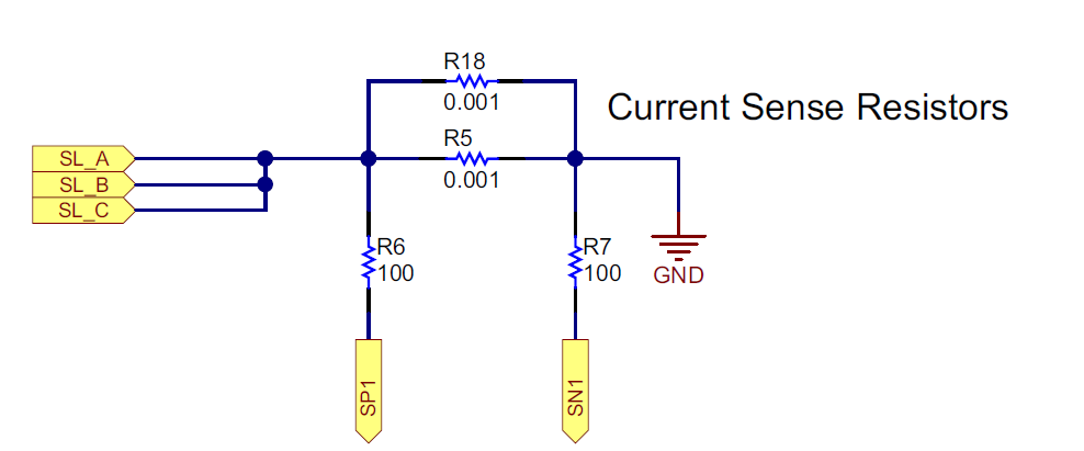
1. What is R11 in the below pic used for? How to determine the value of R11?

2. What's R6 and R7 used for? How to determine the value.

Thanks.

  • Hello Howard,

    For R11/C24, this is a snubber network to reduce spikes/EMI. 

    R6/R7, let me investigate this.

    ~Leonard 

  • Spikes on C24? Why no resistance in series with C19, C20, C21?

    Thanks.

  • Not spikes on C24, spikes on PVDD. The combination of R11/C24 is a snubber/filter.
  • Hi Howard,

    We have notified the author, and should have a response soon.
  • Thanks. By the way, why the DC_FB needs ESD protection? In my mind, the hall signal needs ESD protection because our hand may touch the hall signal input terminal, but the DC_FB does not have the concern.

  • Hi Howard,

    In this circuit R11 and C4 are used as EMI filter at the input. This will help in suppressing any high frequency (a few tens or hundreds of MHz) spikes or ringing in the PVDD line. So it will help in coducted EMI in the high frequency range. You can see that C11 is a very low value ceramic cap (means very low ESR). R11 is used as a current limiter and damper. This should be tuned on application, if you have an EMI concern.

    On the other hand, C19 and C20 are bulk electrolytic capacitors, which will carry majority of your ripple current. You cannot add a resistor in series with this,that will add as ESR and heats up, and also it reduces the effectiveness of the bulk capacitor. In short C19 and C20 helps in low frequency filtering (power frequency and switching frequency), C21 helps in medium frequecy filtering and C24 helps in high frequency filtering.

    For the question related to R6 and R7:

    There is a capacitor connected between SP1 and SN1 nets (C10 in the schematic). Here we are doing differetial current sensing using a difference amplifier. R6, R7, C10 forms a high frequency RC filter. By putting equal resistance in the positive and negative sensing lines(SP1 & SN1), the effect of opamp bias current gets cancelled. Also we want to measure exactly across the sense resistor. So if we dont have R7 then we will mix up with the ground reference. Please look at the layout of TIDA-00771 avaialable at www.ti.com/.../tida-00771

    For the question related to ESD:

    You are right, we need the ESD protection on the hall sensor and ESD protection maynot be required on the VDC sensing line. But if the track length of VDC sensing line is more, it may capture noise which can enter the MCU pin, where the VDC sense line is connected. We can connect a fast signal diode which clamps to 3.3V for this purpose instead of ESD.

    Regards,
    Manu
  • Hi Manu,

    for the current sense, we have already added a RC filter at the input of the amplifier with R6,R7,C10.

    So why we still need R22 and C11 between IDC and MCU? How to determine the value of R22 and C11?

    Thank you.