This thread has been locked.

If you have a related question, please click the "Ask a related question" button in the top right corner. The newly created question will be automatically linked to this question.

DRV8350: First design and use DRV8350, Please help on reviewing and some questions.

Part Number: DRV8350

Hi, 

My customer is the first time to use DRV8350H,so am I.  please help to review their schematic and some questions.

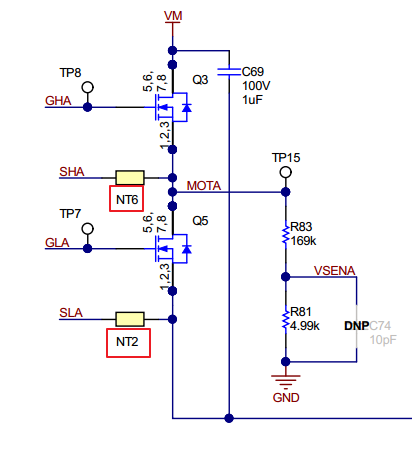
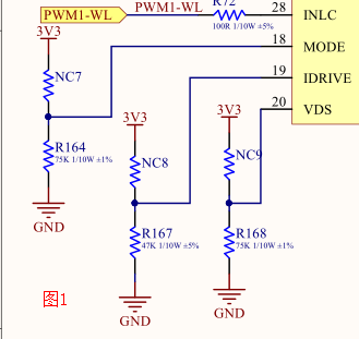
the schematic is as attached.

Gate Drive Regen.pdf

Q1:Please  recommend the suitable component for pin 18,19 and 20  according to the used MOSFET [IPD60N10S4L-12

BTW, it would be great if can also help to suggest suitable component for TI MOS CSD19533KCSIPD60N10S4L-12.pdf

Q2:Without any external OCP detect circuit, please confirm is it enough and safe to just use the internal overcurrent and Short Circuit.

  • Yue,

    Schematic feedback:

    1.  The VCP capacitor is incorrect, this cap must be connected from VCP to VDRAIN and it should have a 100V rating.
    2.  Please also make the CPH/CPL capacitor 100V rated.
    3.  Pin 18 is the MODE pin, the selection of this pin depends on the customer's need, will the customer be using 1X, 3X, or 6X PWM? Currently the 75l they have there is not valid for any mode.
    4.  Pin 19 is the IDRIVE pin, based on the FET mentioned, they should use the lowest IDRIVE setting which means pulling IDRIVE pin to GND directly. They should include a 0 ohm resistor in case this needs to be changed later.
    5. Pin 20 is the VDS pin, this must be decided by the customer. The RDSON of the FET is 12mOhms. Once the customer knows their expected current limit they can calculate the associated VDS limit and program the DRV so that the device will protect above this current limit.
      1. VDS limit = (FET CURRENT) x (RDSON)
    6. The gate resistors and diode are not needed when using Smart Gate Drive and IDRIVE, I would remove these components.
    7. Please make sure that the SLA/SLB/SLC pins are routed to the Low-Side FET Source directly and not the board GND plane. You can check the DRV8350 EVM for an example.

    FET selection will control the selection of IDRIVE and customer must select appropriate VDS for their application. MODE is not dependent on FET selection.

    IDRIVE for CSD19533: Pull IDRIVE to GND through 0 ohm. This FET has very small QGD so gate resistance may be needed if FET gate and source are ringing. 

    The DRV8350 has VDS protection which will help cover OCP and short circuit protection. The device also has VGS protection to ensure that each FET is OFF or ON only when intended. For most customers this is enough coverage.

    Regards,

    -Adam

  • Thanks for the review, it is very helpful.

    one more question about our EVM design, what is below NTx(red box) stand for? 

  • This means Net Tie which is used to connect two differently named nets, it is schematic only, no effect on the PCB or layout.

    Regards.

    -Adam