This thread has been locked.

If you have a related question, please click the "Ask a related question" button in the top right corner. The newly created question will be automatically linked to this question.

DRV3245Q-Q1: What is the trigger to activate the VDS/VGS monitor?

Part Number: DRV3245Q-Q1

Hello Team,

I'm Yuta Kurimoto from TIJ.

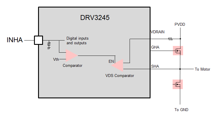
Now our customer has been evaluation DRV3245AQ-Q1. They have a question about the trigger which activates the VDS/VGS monitor.

Datasheet says "The tBLANK time is inserted after each switch-on transition (LOW to HIGH) of the output gate drivers is commanded.", but they don't know how to interpret this.

Q. What is the trigger to activate the VDS/VGS monitor?

For example, they are guessing the trigger is

- DRV3245-Q1 monitors the INH/INL PWM signal by internal comparator. When the INH/INL turns to HIGH, it will trigger to activate the VDS/VGS monitor.

- DRV3245-Q1 monitors the state of internal push-pull stage by comparator. When the high side FET of the push-pull turned ON, it will trigger to activate the VDS/VGS monitor.

- DRV3245-Q1 monitor the Gate voltage(w.r.t  the Source) for external FET. When the gate voltage exceed some threshold, it will trigger to activate the VDS/VGS monitor.

Thanks,

Yuta Kurimoto

  • Hi Kurimoto-san,

    When the external MOSFET is first turned on or off, the Vgs and Vds of the MOSFET will take some time to change as the gate is charged/discharged.

    In order to avoid triggering the Vds/Vgs monitors every time the output switches, the DRV3245 will ignore the output of the Vds and Vgs monitors for the "tBLANK" period after a rising/falling edge of the INH/INL pins. Once tBLANK has expired, if the drain-source or gate-source voltages exceed the threshold for more than the deglitch period, then the DRV3245 will set the VDS/VGS fault flag.

    Thanks,

    Garrett

  • Hello Garrett,

    Thanks for your answer.

    I know the meaning of "blanking time" and "deglitch time" and the reason why it is implemented.

    What I want to know is little bit different.

    In my understanding, the Both VDS comparator and VGS comparator are desabled during the external FET is OFF state, otherwise these comparators will detect VGS_TRIP_L and VDS_TRIP by mistake.

    Therefore I think these VDS comparator and VGS comparator are enabled  only during the external FET is ON state. I want to know what is the trigger to "enable" the VDS/VGS comparator.

    Thanks,

    Yuta Kurimoto

  • Hi Kurimoto-san,

    Ah, I understand now.

    The VGS monitor actually detects two conditions. When INHx/INLx is low, the MOSFET should be off, so it monitors to make sure Vgs is not too high. When INHx/INLx is high, the MOSFET should be on, so it monitors to make sure Vgs is not too low. So VGS monitors are enabled whenever gate drive output is enabled.

    However, the VDS monitor is only enabled while INHx/INLx is high (when gate drive output is enabled).

    Thanks,

    Garrett

  • Hello Garrett,

    I understood about the VGS monitor. Thanks.

    Regarding with the VDS monitor, below is my understading. Is it correct?

    Sub comparator monitors the INHA voltage ⇒ When the INHA voltage is HIGH, the sub comparator output ENABLE signal for VDS comparator.

    Thanks,

    Yuta Kurimoto

  • Hello Garrett,

    How about the your answer?

    Thanks,

    Yuta Kurimoto

  • Hi Kurimoto-san,

    There is no special sub-comparator just for enabling/disabling the VDS monitor, it runs on the same digital input signals as the rest of the device's functions related to INHx/INLx pins. Other than that, your understanding is correct.

    Thanks,

    Garrett