This thread has been locked.

If you have a related question, please click the "Ask a related question" button in the top right corner. The newly created question will be automatically linked to this question.

BOOSTXL-DRV8323RS: UVLO Fault

Part Number: BOOSTXL-DRV8323RS


Hi, I recently purchased a DRV 8323RS Booster Board to run an FOC algorithm (3x PWM mode) using a Tiva C MCU (80MHz system clock) and an absolute position magnetic encoder. I am testing my algorithm on a hobby brushless motor DYS D2836 (~91mili ohms phase resistance, ~11uH phase inductance, and 0.001 Wb phase flux linkage, 7 pole pairs). PWM frequency is 5kHz (up-down counting) and VM is 15V, amplifier gains are set to 40V/V and the sampling is synchronized with the PWM (i.e. interrupt when PWM counter of phase A = 0, or LS gates are ON and HS gates are OFF) and all 3 generators are center aligned. TDRIVE is set to 2000ns and TDEAD to 400ns, HS gates set to 60mA for a rise time of ~100ns and LS gates 120mA for a fall time of ~50ns. I've checked the math of my FOC loop and it works fine. Current and position sensors outputs scale appropriately.

Problem: I'm using a switching power supply for my VM of 15VM. As soon as I run my algorithm I keep getting UVLO faults and my power supply dumps a lot of current (e.g. reaching the limit of my supply of ~5A). Based on the data sheet regarding Power Supplies, this failure seems to fit a low bulk capacitance problem. I think my bulk capacitance was not high enough (e.g started with a single 100uF electrolitic cap between power and ground), but the problem continued. Thus,  I've added five 10uF electrolitic and five 22uF  electrolitic capacitors between power and ground of my power supply to increase the capacitance, but I keep getting the same UVLO fault, the same large amount of current, and VM drops by 7V.

Questions:

1. Could this fault damage the Driver and/or mosfets?

2. How can I properly size caps for bulk capacitance?

3. Do you think the root cause is related to a different topic and not bulk capacitance?

  • Andres,

    Thanks for posting on the MD forum!

    Do you have a bench lab power supply that you can try? I'm wondering if the supply you are using is fast enough to keep up with the current demand.

    Have you checked section 10.1 (Bulk Capacitance Sizing) in the datasheet?

    Regards,

    -Adam

  • Hi Adam, thanks for the follow. This is the power supply I have:

    15SDS019-3010D-09.V1

    I got this from Amazon, so not sure if from the specs you could tell if this supply is suitable for this application; the current can still go up to 10A, but I'm hesitant on increasing the current. Could you recommend one so that I can check it out? Also, I did check section 10.1 but the data sheet states that bulk cap sizing is setup dependent, so not sure from a design perspective how to derive the capacitance that is needed to prevent ~50% voltage drop.

    Thanks

  • Andres,

    Could you explain why your PWM frequency is so low? 5kHz seems too low and may cause issues. You could try doubling it and checking if it helps the issue.

    Do you have an oscilloscope that you can use to check the VM voltage near the DRV?

    Regards,

    -Adam

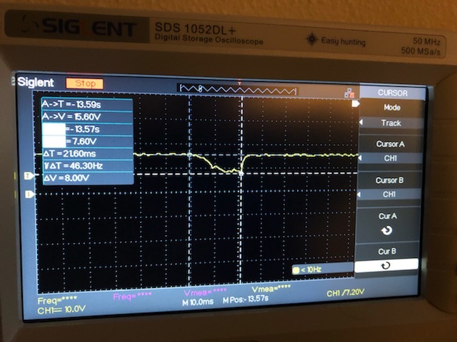
  • Hi Adam, I started with 10kHz PWM frequency (or FOC sampling rate) but encountered this UVLO fault. I thought a lower sampling rate could fix this problem, but I saw no change. Below is a figure of the voltage drop. Note that once the MCU reads the UVLO fault I set the duty cycle of all three generators to zero, which is why you can see a fast voltage increase to nominal. In this figure I'm probing VM power to ground.

    Do you think this problem could be related to the starting sequence in firmware? The enable pin of the DRV is also connected to the low side gates of the DRV. So the first line of my firmware is the programming of my IO ports and then enabling the DRV pin. Afterwards I program the DRV registers: DCR, CSACR, OCPCR, HSR & LSR. Lastly I program my PWM module and enable the PWM counter interrupts.

    Could I get your thoughts on other things that I could try?

  • Andres,

    I didn't get any image above, could you repost it?

    Regards,

    -Adam

  • Hi Adam, thanks for the follow up. I'm sorry I think the image did not upload correctly the first time, so I've uploaded the image again. Let me know your thoughts.

  • Andres,

    Do you know the start-up current requirement of your motor under your load conditions?

    It's hard to debug this remotely as I don't know your algorithm or motor.

    Regards,

    -Adam

  • Hi Adam, below is my hardware config:

    init_DRV(); // there's a 60ms delay inside this function for DRV enable

    // Driver control register
    DRV_Write( DCR ,( (PWM_MODE_3X<<5) | (CLR_FLT) ) );

    // Current sense amplifier control register
    DRV_Write( CSACR ,( (VREF_DIV_BI<<9) | (CSA_GAIN_40<<6) | (CSA_CAL_A_EN<<4)| (CSA_CAL_B_EN<<3) | (SEN_LVL_1V) ) );
    for (ccc = 1; ccc <= 300000; ccc++) // add delay

    DRV_Write( CSACR ,( (VREF_DIV_BI<<9) | (CSA_GAIN_40<<6) | (CSA_CAL_A_DIS<<4)| (CSA_CAL_B_DIS<<3) | (SEN_LVL_1V) ) ); // disable CSA_CAL pins to finish calibration protocol

    // Overcurrent protection control register
    DRV_Write( OCPCR ,( (TRETRY_50US<<10) | (DEAD_TIME_400NS<<8) | (OCP_MODE_RETRY<<6) | (OCP_DEG_8US<<4) | (VDS_LVL_1_88V) ) );


    // Gate Drive high side control register
    DRV_Write( HSR ,( (IDRIVEP_HS_820MA<<4) | (IDRIVEN_HS_1140MA ) ) );

    // Gate Drive low side control register
    DRV_Write( LSR , ( (TDRIVE_2000NS<<8) | (IDRIVEP_LS_440MA<<4) | (IDRIVEN_LS_660MA)) );


    Init_GPIO(); // PB1(toggle pin) used to measure FOC computations on oscilloscope
    init_HES(); // PB7,PB6,PB5,PB4 (SPI for hall effect sensor)
    Init_ADC(); // PE0,PE1 (current sampling) (ADC)
    InitPWM(); // PC4,PC5,PE4 (PWM)

    // Globally enable the interrupts
    __enable_irq();

    Here is my InitPWM() function:

    // PC4,PC5,PE4 (Module 0 PWM5)
    // 0. enable the clock to the PWM module (PWM0)
    HWREG(SYSCTL_RCGCPWM) |= SYSCTL_RCGCPWM_R0;

    // 1. enable the clock to Port C & E
    HWREG(SYSCTL_RCGCGPIO) |= ( (SYSCTL_RCGCGPIO_R2) | (SYSCTL_RCGCGPIO_R4) );

    // 2. select the PWM clock as system clock
    HWREG(SYSCTL_RCC) = (HWREG(SYSCTL_RCC) & ~SYSCTL_RCC_PWMDIV_M );

    // 3. make sure that the PWM module clock has gotten going
    while( (HWREG(SYSCTL_PRPWM) & SYSCTL_PRPWM_R0) != SYSCTL_PRPWM_R0)
    ;
    // 4. disable the PWM while initializing
    HWREG(PWM0_BASE+PWM_O_3_CTL) = 0;
    HWREG(PWM0_BASE+PWM_O_2_CTL) = 0;

    // 5. program generators to go to 1 at rising compare A/B, 0 on falling compare A/B
    HWREG(PWM0_BASE+PWM_O_3_GENA) = (PWM_3_GENA_ACTCMPAU_ONE|PWM_3_GENA_ACTCMPAD_ZERO);
    HWREG(PWM0_BASE+PWM_O_3_GENB) = (PWM_3_GENB_ACTCMPBU_ONE|PWM_3_GENB_ACTCMPBD_ZERO);
    HWREG(PWM0_BASE+PWM_O_2_GENA) = (PWM_2_GENA_ACTCMPAU_ONE|PWM_2_GENA_ACTCMPAD_ZERO);

    // 6. Set the PWM period. Since we are counting both up & down, we initialize
    // the load register to 1/2 the desired total period. We will also program
    // the match compare registers to 1/2 the desired high time
    HWREG(PWM0_BASE+PWM_O_3_LOAD) = ((PeriodInUS * PWMTicksPerUS))>>1;
    HWREG(PWM0_BASE+PWM_O_2_LOAD) = ((PeriodInUS * PWMTicksPerUS))>>1;

    // 7. Set initial DC to zero
    // ************************
    HWREG(PWM0_BASE+PWM_O_3_GENA) = PWM_3_GENA_ACTZERO_ZERO;
    HWREG(PWM0_BASE+PWM_O_3_GENB) = PWM_3_GENB_ACTZERO_ZERO;
    HWREG(PWM0_BASE+PWM_O_2_GENA) = PWM_2_GENA_ACTZERO_ZERO;
    //*************************

    // 8. enable the PWM outputs
    HWREG(PWM0_BASE+PWM_O_ENABLE) |= (PWM_ENABLE_PWM4EN | PWM_ENABLE_PWM6EN | PWM_ENABLE_PWM7EN);
    // 9. now configure the Port pins to be PWM output
    // start by selecting the alternate function
    HWREG(GPIO_PORTC_BASE+GPIO_O_AFSEL) |= (BIT4HI | BIT5HI); //PC4 & PC5
    HWREG(GPIO_PORTE_BASE+GPIO_O_AFSEL) |= (BIT4HI); // PE4
    // 10. now choose to map PWM to this pin, this is a mux value of 0 that we
    // want to use for specifying the function on bit 0 (page 688 & 1351)
    HWREG(GPIO_PORTC_BASE+GPIO_O_PCTL) = (HWREG(GPIO_PORTC_BASE+GPIO_O_PCTL) & 0xff00ffff) + (4<<(4*BitsPerNibble)) + (4<<(5*BitsPerNibble));
    HWREG(GPIO_PORTE_BASE+GPIO_O_PCTL) = (HWREG(GPIO_PORTE_BASE+GPIO_O_PCTL) & 0xfff0ffff) + (4<<(4*BitsPerNibble));
    // 11. enable pins 4 & 5 on Port C & pin 4 on port E for digital I/O
    HWREG(GPIO_PORTC_BASE+GPIO_O_DEN) |= (BIT4HI | BIT5HI);
    HWREG(GPIO_PORTE_BASE+GPIO_O_DEN) |= (BIT4HI);
    // make pins into outputs
    HWREG(GPIO_PORTC_BASE+GPIO_O_DIR) |= (BIT4HI | BIT5HI);
    HWREG(GPIO_PORTE_BASE+GPIO_O_DIR) |= (BIT4HI);
    ///////////////////////////////////////////////////
    // Registers for interrupt enable
    // Enable PWM interrupt on PWM Generator 3
    HWREG(PWM0_BASE+PWM_O_INTEN) |= PWM_INTEN_INTPWM3;// interrupt enable globally on generator 3 from module 0
    HWREG(PWM0_BASE+PWM_O_ISC) |= PWM_ISC_INTPWM3; // interrupt status clear
    HWREG(PWM0_BASE+PWM_O_3_INTEN) |= PWM_3_INTEN_INTCNTZERO; // enable interrupt when counter = 0
    HWREG(PWM0_BASE+PWM_O_3_ISC) = PWM_3_ISC_INTCNTZERO; // clear the source of the interrupt

    //page 134 (table 2-9 page 104)
    // PWM3, interrupt number 45, so bit 13 on EN1
    HWREG(NVIC_EN1) = BIT13HI;
    /////////////////////////////////////////////////////

    // set the up/down count mode, enable the PWM generator
    // and make both generator updates locally synchronized to zero count
    HWREG(PWM0_BASE+PWM_O_3_CTL) = (PWM_3_CTL_MODE | PWM_3_CTL_ENABLE | PWM_3_CTL_GENAUPD_LS | PWM_3_CTL_GENBUPD_LS); 
    HWREG(PWM0_BASE+PWM_O_2_CTL) = (PWM_2_CTL_MODE | PWM_2_CTL_ENABLE | PWM_2_CTL_GENAUPD_LS); 

    }

    Below is my current FOC algorithm:

    A few notes:

    1) PWM clock is at 80Mhz (or 12.5ns resolution) and frequency is set at 20kHz

    2) VM is 15V

    3) IQ = 0.5A and ID = 0A. Reference for PI loops

    4) Max DC is 70% since my current sampling take ~3.5us and 70% DC is the max I can achieve in order to ensure that I'm sampling when the high gates are OFF and low gates are ON. Min DC is 5%

    5) Total FOC algorithm takes ~22.5us (note that PWM period is 50us)


    #define NPP 7.0f // number of pole pairs
    #define AMPS_PER_COUNTS 0.002876869965f // Using Gain of 40V/V
    #define RADS_PER_COUNTS 0.000383495197f //
    /////////////////////////////////////////////
    #define LOOP_PERIOD 0.00005f // 1/20kHz
    #define PWMTicksPerUS 80/1 // SysClk/1
    #define PeriodInUS 50
    #define DC_MAX 0.70f
    #define DC_MIN 0.05f
    static float v_bus = 15.0f;
    static float iq_ref = 0.5f, id_ref = 0.0f;
    //////////////////////////////////////////////
    static float pGain = 0.086f, iGain = 0.334f; // 20kHz sampling frequency
    static float iq_error = 0.0, id_error = 0.0;
    static float thetadot_mech = 0;
    static float vq_cmd, vd_cmd;
    static float cmd_mag;
    static float dc_u,dc_v,dc_w;
    static float theta_mech = 0;
    static uint16_t HES;
    static float i_a = 0.0,i_b = 0.0,i_c = 0.0;
    static uint32_t c_a,c_b,c_c;
    static float q_int = 0.0,d_int = 0.0;
    static uint32_t Current[2];
    static float i_d = 0.0,i_q = 0.0;
    static float cf = 0.0,sf = 0.0;
    static float v_offset = 0.0;
    static float v_u = 0.0f,v_v = 0.0f,v_w = 0.0f;

    void SampleISR( void )
    {
    // 1. === Clear the source of the interrupt ===
    HWREG(PWM0_BASE+PWM_O_3_ISC) = PWM_3_ISC_INTCNTZERO;

    // 2. === Analog read current sensor pins ===
    ADC_MultiRead(Current); // this function takes 3.5us to complete

    c_a = Current[0];
    c_b = Current[1];

    i_a = (REF_COUNT-(float)c_a)*AMPS_PER_COUNTS;
    i_b = (REF_COUNT-(float)c_b)*AMPS_PER_COUNTS;
    i_c = -i_a-i_b;

    // 1. === Analog read position sensor pin ===
    SampleThetaMech();
    theta_mech =(float)HES*RADS_PER_COUNTS;

    // 3. === Calculate dq0 currents ===
    cf = fCos(theta_mech*NPP);
    sf = fSin(theta_mech*NPP);
    i_d = 0.6666667f*(cf*i_a + (0.86602540378f*sf-.5f*cf)*i_b + (-0.86602540378f*sf-.5f*cf)*i_c);
    i_q = 0.6666667f*(-sf*i_a - (-0.86602540378f*cf-.5f*sf)*i_b - (0.86602540378f*cf-.5f*sf)*i_c);

    // 4. === Current controller ===
    id_error = id_ref - i_d;
    iq_error = iq_ref - i_q;

    d_int += pGain*iGain*id_error;
    q_int += pGain*iGain*iq_error;

    // Command voltages
    vd_cmd = pGain*id_error + d_int;
    vq_cmd = pGain*iq_error + q_int;

    // 5. === Limit the desired voltage  ===
    cmd_mag = sqrt(vq_cmd*vq_cmd + vd_cmd*vd_cmd); 
    if(cmd_mag > v_bus){
    vd_cmd = vd_cmd*(v_bus/cmd_mag);
    vq_cmd = vq_cmd*(v_bus/cmd_mag);
    }

    // 6. === ABC Transform ===

    v_u = cf*vd_cmd - sf*vq_cmd;
    v_v = (0.86602540378f*sf-0.5f*cf)*vd_cmd - (-0.86602540378f*cf-0.5f*sf)*vq_cmd;
    v_w = (-0.86602540378f*sf-0.5f*cf)*vd_cmd - (0.86602540378f*cf-0.5f*sf)*vq_cmd;

    // 7. === Space Vector Modulation ===
    v_offset = 0.5f*( fminf3(v_u,v_v,v_w) + fmaxf3(v_u,v_v,v_w) );

    dc_u = fmaxf(fminf( (0.5f + 0.5f*((v_u - v_offset)/v_bus)),DC_MAX),DC_MIN);
    dc_v = fmaxf(fminf( (0.5f + 0.5f*((v_v - v_offset)/v_bus)),DC_MAX),DC_MIN);
    dc_w = fmaxf(fminf( (0.5f + 0.5f*((v_w - v_offset)/v_bus)),DC_MAX),DC_MIN);

    // 8. === Set DC ===
    HWREG(PWM0_BASE+PWM_O_3_CMPA) = (HWREG(PWM0_BASE+PWM_O_3_LOAD)) - ((PeriodInUS * PWMTicksPerUS)*(dc_u))/2;
    HWREG(PWM0_BASE+PWM_O_3_CMPB) = (HWREG(PWM0_BASE+PWM_O_3_LOAD)) - ((PeriodInUS * PWMTicksPerUS)*(dc_v))/2;
    HWREG(PWM0_BASE+PWM_O_2_CMPA) = (HWREG(PWM0_BASE+PWM_O_2_LOAD)) - ((PeriodInUS * PWMTicksPerUS)*(dc_w))/2;

    }

    Below, the yellow probe is VM and the purple probe is the high side source MOSFET of MOTC on the DRV8323RS boostxl. Note that this dip in VM is causing the UVLO fault. For this sensored FOC implementation, is it necessary to implement a ramp in DC?

  • Andres,

    It looks to me that your power supply is not fast enough or it cannot provide enough instant current to maintain the VM voltage. 

    I would try another power supply or ramp the current slower.

    Unfortunately I cannot review code posted on E2E.

    Regards,

    -Adam