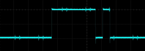
Dear colleagues,
Our customer is using several DRV8860/ board. When they combine 2 DRV8860 to test. They find a strange issue. In their real usage, DRV8860 works alone.

Test progress:
(1) By writing "1" to the data register of A and B DRV8860 at the same time, the OL bit of fault register is cleared (at this time, the OL bit is read as "0"). Then write the data register "0" to turn off the out output of DRV8860.
(2) Read the fault register of drv8860 respectively. It is found that the read values are different. The chip A reads 0x00ff and the chip B reads 0x0000. Due to the existence of a 5V pull-up, reading to 00 is normal. It is detected that the nFault pin of chip A DRV8860 becomes low level, and the nFault pin of chip B remains the high level.
(3) Just connect chip A out1 and chip B out1. Repeat (1),(2), when reading the fault register, grab the output waveform of Dout pin. From the waveform, it can be seen that the chip A fault register OL is set to "1" again, while the chip B fault register OL is not set to "1". The voltage of output out1 of A and B are 5V.
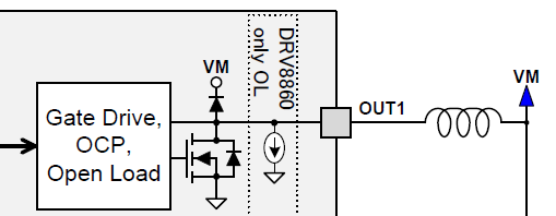
Chip A, turn on out1, read Fault register, Dout waveform:
Chip A, turn off out1, read Fault register, Dout waveform:
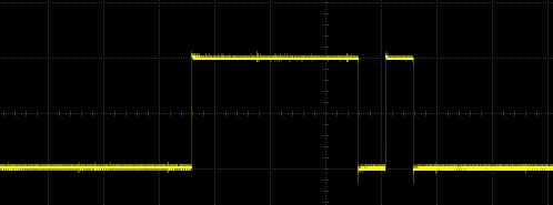
Chip B, turn on out1, read Fault register, Dout waveform:

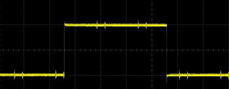
Chip B, turn off out1, read Fault register, Dout waveform:
Note: 1. During the whole test, keep the output terminal pulled up.
2. The output terminal of the single drv8860 is pulled up, and then the fault register is read normally (0x0000).
Question:
1. Can such a test method cause an exception in DRV8860?
2. Can you provide the detailed circuit of DRV8860 OL detection?
3. When using the DRV8860, are there other limitations?
Best Regards,
Rock Su