This thread has been locked.

If you have a related question, please click the "Ask a related question" button in the top right corner. The newly created question will be automatically linked to this question.

DRV8830: Don't be sleep state at DRV8830

Part Number: DRV8830

Hello team,

Customer use DRV8830 but it doesn't move to sleep state when IN1 and IN2 are Low.
Could you estimate a reason?

The situation are;

  • IN1 and IN2 are low state
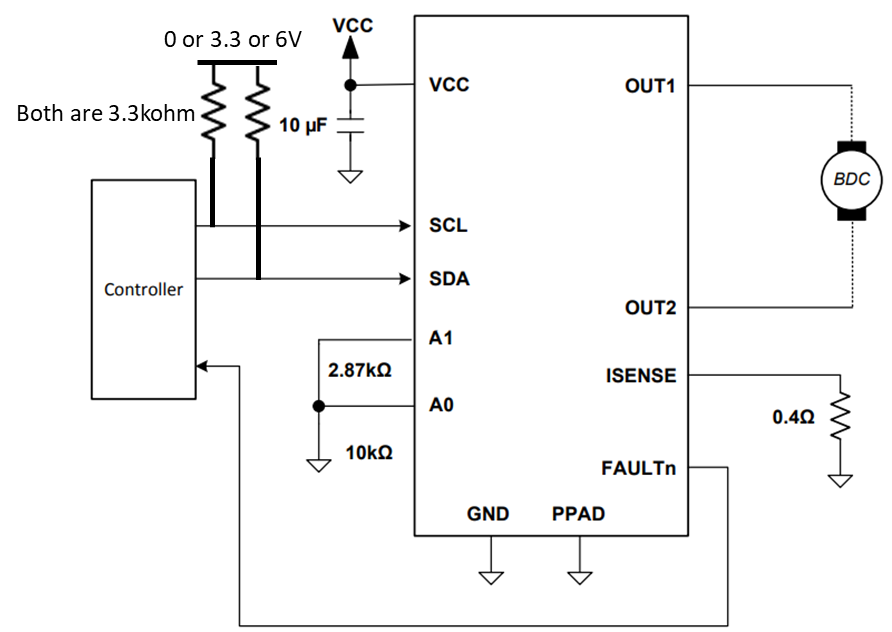
  • Vcc=6V, I2C is 3.3V with pullup resister
  • Motor operation by I2C is fine
  • When applying 3.3V at I2C, the standby current is around 500uA which is out of the spec.
    However, when applying 6V or GND, the standby current is around 0.3uA which is within the spec.
    The voltage and pull up resister is connected like below picture.

Best regards,
Koyo

  • Hi Koyo-san,

    Can the customer provide the measurement for the V_IH (input high voltage) when 3.3V is applied at I2C? The issue could be that the actual input high voltage is less than the V_IH specified in the datasheet which is 0.5*VCC.

  • Hi Pablo,

    The voltage range is Vcc=3.0~6.0V (CR123 series connection) and I2C=3.0~3.3V comes from LDO.
    Therefore I2C voltage don't be less than V_IH (0.5*Vcc).

    Additional info;

    • Other state, forward/reverse/brake, can be operated as expected.
    • When Vcc and I2C are same voltage, this IC can work but standby can't be worked when Vcc and I2C are different voltage.
      (When Vcc=I2C=3.3V or Vcc=I2C=6V, can work but when Vcc=6V and I2C=3.3V, standby can't be worked)

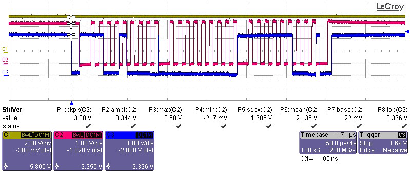
    Followings are waveform of Vcc and I2C.

    Yello: Vcc=6V, Blue: SDA=3.3V, Red: SCL=3.3V

    Could you estimate a reason why this IC can't be standby when IN1 and IN2 are low?

    Best regards
    koyo

  • Hi Koyo-san,

    Let me do more research into this issue and I will get back to you by early next week.

  • Hi Pablo,

    Let me comment additionally.

    They are using own board and 
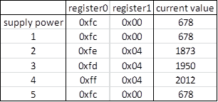
    1 Standby -> 2 CCW -> 3 CW -> 4 Break -> 5 standby are transmitted in this order.
    After the transmitting, read register 0 and 1.
    The flow is like below. (the current units are uA)

    They had written the Firmware to several boards but same issues are observed.

    Best regards,
    Koyo

  • Koyo-san,

    Thanks for the information. As discussed privately, I will close this thread and post again once I obtain an explanation for the issue observed by the customer. We will keep discussion privately.