This thread has been locked.

If you have a related question, please click the "Ask a related question" button in the top right corner. The newly created question will be automatically linked to this question.

DRV8702D-Q1: DRV8702D-Q1: Dead time

Part Number: DRV8702D-Q1

Hi,

I'm trying to get a better understanding of the dead time of the driver.

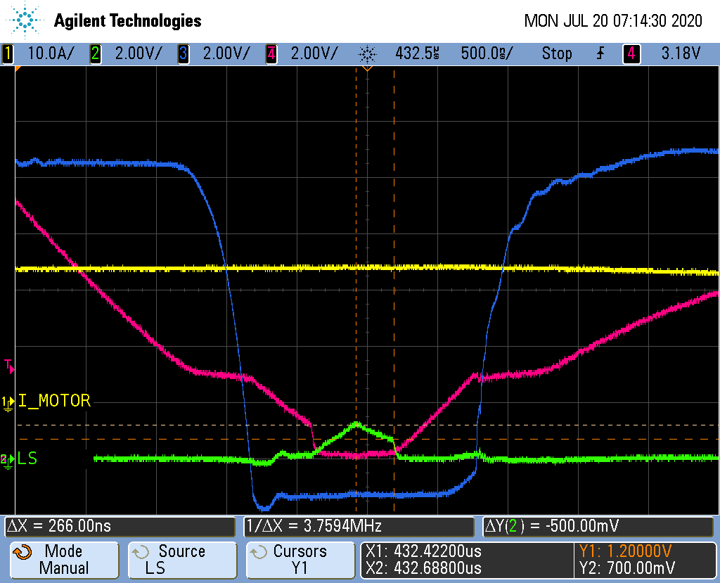
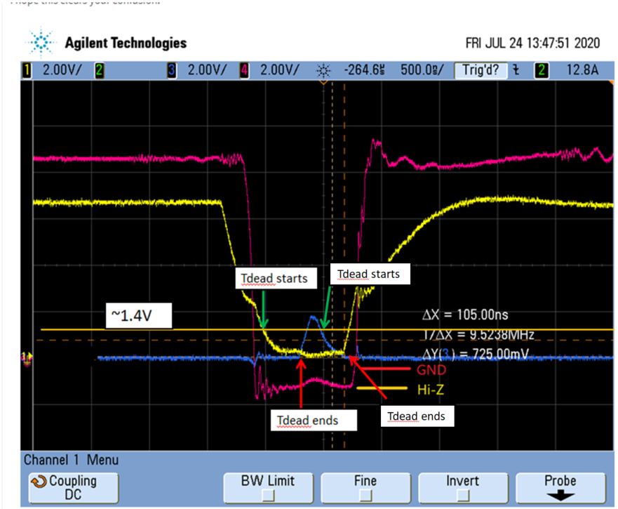
According to data sheet the driver has a digital dead time of ~240ns which starts when the SH pin is in the Hi-Z state (after turning off one mosfet). When does this time start in case of almost 100% pwm, if the low side only switches on for a very short time and SH stays in Hi-Z all the time?

In addition there seems to be another check (FET gate slewing):

"In addition to this digital dead time, the output is Hi-Z as long as the voltage across theGL pin to ground or GH pin to SH pin is less than the FET threshold voltage.

The total dead time is dependent on the IDRIVE resistor setting because a portion of the FET gate ramp (GHand GL pins) includes the observable dead time."

What does it mean "GL to ground"?  Because in my measurement below, the strong pulldown of LS and the turn on of the HS starts before GL reach ground.

What does it mean "GH pin to SH pin is less than the FET threshold voltage" ? How does the Driver detect the threshold voltage of the specific mosfet.

To be able to understand and display this, I have set the switching speed to minimum (IDRIVE on ground):[green=GL; red=GH; blue=SH; yellow= I_Motor]

Best regards

Tobias Schmidt

  • Hi Tobias,

    Let me research this and I will get back to you by 7/21 US time.

  • Hi Tobias,

    [Q] When does this time start in case of almost 100% pwm, if the low side only switches on for a very short time and SH stays in Hi-Z all the time?

    [A] I will need to go to the lab and do more research. I will give you an update by the end of this week.

    [Q] What does it mean "GL to ground"?

    [A] GL to ground refers to the VGS voltage of the LS FET assuming the source of the FET is connected to GND.

    [Q] What does it mean "GH pin to SH pin is less than the FET threshold voltage" ?

    [A] The GH pin to SH pin voltage is the voltage between the gate and source of the HS FET. Usually this voltage along with the VGS of the LS FET is monitored internally via VGS monioring circuitry which is fed to the TDRIVE state machine. I recommend reading this appnote to learn more about smart gate drive. 

  • Hi Pablo,

    I have asked because with the slowest idrive the driver does not wait until Vgs of the other MOSFET is 0V. And I thought the handshake would make sure that.

    And to my first question which one you still look at, I have here again two Pictures (IDRIVE 200k to GND). In the first picture you see an expected dead time and in the second picture this is much shorter.

    Best regards

    Tobias

  • Hi Tobias,

    Thank you for providing the scope shots. 

    Let me first clarify how the handshake mechanism works. In the case of turning OFF the HS FET and turning ON the LS FET, the handshake mechanism will turn ON the LS FET when the VGS voltage of the HS FET is below 1.4V which is the typical VGS threshold for the internal FETs. The handshake does NOT wait until the HS FET VGS voltage reaches all the way to 0V in order to turn ON the LS FET. What you are seeing in your scope shots is normal operation.

    Is the IDRIVE resistor for the last two scope shots the same or is it different? If it is different, then the different dead time is expected. As mentioned on section 7.3.8 of the datasheet, the dead time is dependent on the Idrive resistor setting because a portion of the FET gate ramp (GH and GL pins) includes the observable dead time.

  • Hi Pablo,

    got it. Did you have specified the internal FETs with a max VGS threshold value? Because I'm using external Power FETs with min VGS threshold value of 1.4V.

    No, the IDRIVE resistor for the last two scope shots is the same (200k to GND). The only difference is the duty cycle / the high of LS Vgs. If Vgs only reach < ~2V, the dead time is shorter. In the datasheet is meantioned that "the dead time is measured as the time when the SH pin is in Hi-Z state between turning off one of the half-Bridge FETs and turning on the other."

    Does it mean if SH pin don't reach Hi-Z state completely, that there is no digital dead time (Last scope shot-> blue=VGS-LS / yellow=VGS-HS / red=SH-Pin)? Or at which Point in time does the digital dead time starts to count?

    Best regards

    Tobias

  • Hi Tobias,

    [Q]  Did you have specified the internal FETs with a max VGS threshold value?

    [A] There is no specification for the maximum VGS threshold of the FETs. Since the min VGS threshold of the power FETs you are using is 1.4V, then it should behave properly with the driver.

    [Q] Does it mean if SH pin don't reach Hi-Z state completely, that there is no digital dead time (Last scope shot-> blue=VGS-LS / yellow=VGS-HS / red=SH-Pin)? Or at which Point in time does the digital dead time starts to count?


    [A] Normally, the tdead timer starts when the VGS of the FET drops below ~1.4V. In the case that the VGS is above ~1.4V at the end of TDRIVE,  a gate drive fault is asserted to protect the device from a potential shoot-through condition. So in the case of switching from LS to HS, if the LS FET VGS is above ~1.4V (meaning SH pin does not reach High-Z state), a gate drive fault condition will be triggered and both FETs are disabled to protect the device and the load. To prevent a gate drive fault, you can increase the TDRIVE to allow the LS FET VGS to fully turn OFF. However, with a higher TDRIVE, you run the risk of potential damage to the device if a GL/GH short to GND, VM, or SH occurs before the TDRIVE time is done. A shorter TDRIVE will ensure that the short only persists for s shorter time before the gate drive fault is asserted

    I hope this answers your question.  

  • Hey Pablo,

    sorry my fault. I have described it wrong.

    I meen in my case the VGL (blue) turns on only a short time and the SH Pin (red) does not come out of the Hi-Z state (to GND) than the dead time is much shorter. When does here the dead time start to Count?

    by comparison with the longer dead time:

    Thank You.

    Best regards

    Tobias

  • Hi Tobias,

    Thank you for the clarification. 

    To answer your question, I have made some drawings on your scope shot. The tdead timer will start when GH is approximately equal to 1.4V and timer will stop when the tdead expires. In total, tdead will consist of the digital dead time of 240ns plus additional time that is present in the FET gate slewing. Therefore, adjusting IDRIVE will change the dead time since the time portion of the FET gate slewing will be changing.

    In the case of the scope shot below, GL (blue line) starts turning on after tdead expires but since the duty cycle is so high, the next PWM cycle begins before there was enough time for the LS FET to turn on and pull SH out of High-Z to GND. If you compare this scope shot with lower duty cycle scope shot (shown below), the lower duty cycle allowed the LS FET to turn on before the next PWM started. In any case, both plots have around the same Tdead however, the one with higher duty did not have enough time to bring SH to GND and that made it seem like the dead time is longer. 

    I apologize if the definition of Tdead described in the datasheet caused your confusion.

    I hope this clears your confusion. 

  • Hi Pablo,

    I'm sorry to be so persistent.

    All dead times you marked are understandable. I am specifically interested in what the driver is doing in the circle marked in red, where you didn't marked any dead time.

    At the orange line the input of the driver says to switch on the HS. After this orange line you didn't mark dead time, but the Driver turn off the GLS and wait a bit (which is good because the LS-FET is already in a swiching state/above the VGS(th)) until he turns on the HS. This time Looks smaller than the other dead times. What is this for a time and what influences this time? I want to be sure that the HS-FET does not switch on if the LS-FET is still in some switching state?

    Thanks for your perseverance with me.

    Best regards

    Tobias

  • Tobias,

    Thank you for the clarification. I understand your question now. 

    Let me research this and I will get back to you with a reply by the end of the day 7/31 US time.

  • Hi Tobias,

    I am sorry for the late reply.

    Below is the scope shot showing the start and end of the dead time. The dead time starting when GL (blue) drops below 1.4V and ending when GL begins to rise is slightly smaller than the previous dead time. Normally, the dead time will vary slight depending on different factors. One such factor is the Miller charge (QGD) or the Gate-to-Drain charge. The FET output (SH) is slewing during QGD charge. If any of the internal parasitic capacitance of the FETs varies, the QGD charge time will vary which will affect the dead time. Other factors like PCB trace parasitics could also affect the dead time.