This thread has been locked.

If you have a related question, please click the "Ask a related question" button in the top right corner. The newly created question will be automatically linked to this question.

DRV8816: behavior of the enable pin connected with nFault

Part Number: DRV8816

Hi

I tried to extend the 1,6 ms tOCP Time by connecting the nFault pin to the enable2 pin.
These both pins are connected directly. To realice the default High level I made a resistor divider with 15K against 24V and 3K3 to GND.
To realice the timing I added two 1µF capacitors parallel to the 3K3.

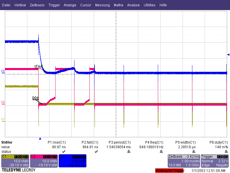
If i scope the two 24V outputs and the nFault/enable2 pin I´ve get this sketch.

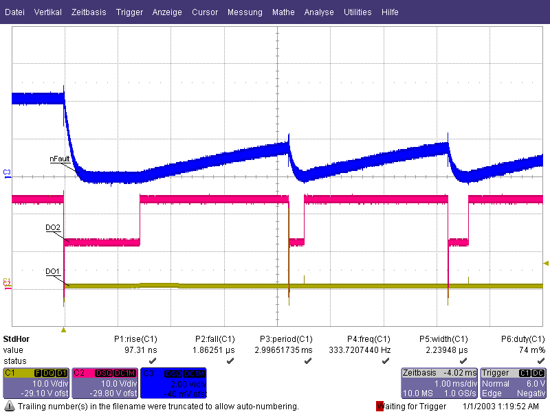
Output 2 drives against an 2*470 Ohm resistor divider at 24V. It looks like that the Output is active as soon as there is any Voltage at the enable2 pin. This differs from the datasheet.
Can somebody explain that?

Kind regards

Thomas

  • Thomas,

    On the waveform, which one is the Enable2 signal? What do DO1 and DO2 mean?

  • Hi Wang

    nFault is directly connected with EN2, so the blue signal represents both.
    DO1 and DO2 arte the both Outputs of the of the DRV8816. DO1 (Output1) is externaly shortet to generate a fault.

    Kind Regards,

    Thomas

  • Thomas,

    The OCP deglitch time is only 3us. I think it matches "the Output is active as soon as there is any Voltage at the enable2 pin". If you zoom in that edge, it should be 3us.

  • Hi Wang

    The logic low level is described for the enables like following:

    In my opinion the outputs must be deactivated (minimum) as long as the voltage at the enable pin is below 0,8V.
    But the Output becomes aktiv as soon as the Fault/Enable 2 leaves the 0V line.

    Kind regards

    Thomas

  • Thomas,

    "Output 2 drives against an 2*470 Ohm resistor divider at 24V".

    Now, understand the output connection and your question. I thought the output was pulled up to 24V before.

    Do you put a series resistor between nFault and EN2? If no, can you disconnect nFault and EN2; just check EN2 input logic low voltage threshold?

  • Thomas,

    Do you have any update on this issue?

  • Wang,

    I have a little update.
    I made a little mistake, for a better layout I switched the both Signales IN1&OUT1 with IN2 & OUT2.
    But at customer side of view OUT2 is DO1 and OUT1 is DO2 (osci picture above).
    So nFault I disable DO1 through the shortcut.

    Now my picture make more sense for me.
    But this brings me to an other question. Is the Tocp time a individual free running timer for every output?
    Because I get different phase positions of the enable time für bothe outputs at every new scope picture I generate.

    Kind Regards


    Thomas D.

  • Thomas,

    Great! You found the root cause.

    I would think tocp timer should be same for all the channels. But, the each input channel's logic high threshold could be have some tolerance.

  • Sorry you didn't answer my question.
    Are there individual free running counters for both Outputs, because of the different phases between the enable time?

    Kind regards.

    Thomas

  • Thomas,

    In the beginning, the goal is "extend the 1,6 ms tOCP Time by connecting the nFault pin to the enable2 pin". Did it work after you fixed the layout?

    I would think the different phases between the enable time is reasonable to DRV8816 due to each input channel's logic high threshold could have some tolerance. If that makes the individual free running counters not work, we may have to redesign the free running counters. What is the new question?

  • Hi
    The high threshold couldn´t be the reason for the phases between the enable time for both channels.
    I made several pictures. In all cases I shortcut the DO2 to GND.

     You You can see that the reactivation of DO1 is always at different levels of nFault(= EN2).
    This let me asume there a two internel free running counters inside the DRV8816 to manage the tOCP Time for each Output.

    So I think the Enable should be at high Level AND the timer counted down the 1,6 ms to reactivate the Output. Is this right?


    Kind regards
    Thomas

  • Thomas,

    According to your test waveform, I agree with you: there a two internel free running counters inside the DRV8816 to manage the tOCP Time for each Output.

    I am trying to understand "the Output is active as soon as there is any Voltage at the enable2 pin." Do you put a load between DO1 and DO2? When DO2 output is HiZ, but DO2 may be pulled up by the load.  

  • Hi

    Do1 is driving against an resitor devider (2*470 Ohm).
    But additionaly to the protection the DRV8816 has we also has an PTC in the supply voltage.
    I think the curves in picture 1 came from this PTC.
    DO2 is directly enabled if nFault isn´t pulled down any longer.

    Kind regards

    Thomas