This thread has been locked.

If you have a related question, please click the "Ask a related question" button in the top right corner. The newly created question will be automatically linked to this question.

DRV8886: what is the root cause why DVDD pin output only 1.5v and AVDD pin output remain 0v?

Part Number: DRV8886
Other Parts Discussed in Thread: MSP430F2617, , MSP430F2416, MSP430F2618, MSP430F2417, UNIFLASH, MSP-FET

Hi ,

I design a PCB with modify the DRV8886 EVM with almost same schematics for DRV8886  driving area except adding one more step down voltage regulator for MSP430F2617 power supplies,

when prototype PCB soldering  all components on itself,I tested and found DRV8886 nFault pin keep logic low, cause alarm LED keep light on , during check the state of  each pin ,I found the Pin of DVDD and AVDD pin voltage level quite abnormal compared  normal state present in DRV8886EVM manual; I don't know why this happen although verify the soldering quality  no obvious problem .

also met one issue when downloading program to msp430f2617TPM, software always post out alarm for the chip is msp430f2416 .something is wrong for my understanding , also attached alarm message. msp430f2617 order while display as MSP430f2416 when download.pdf 

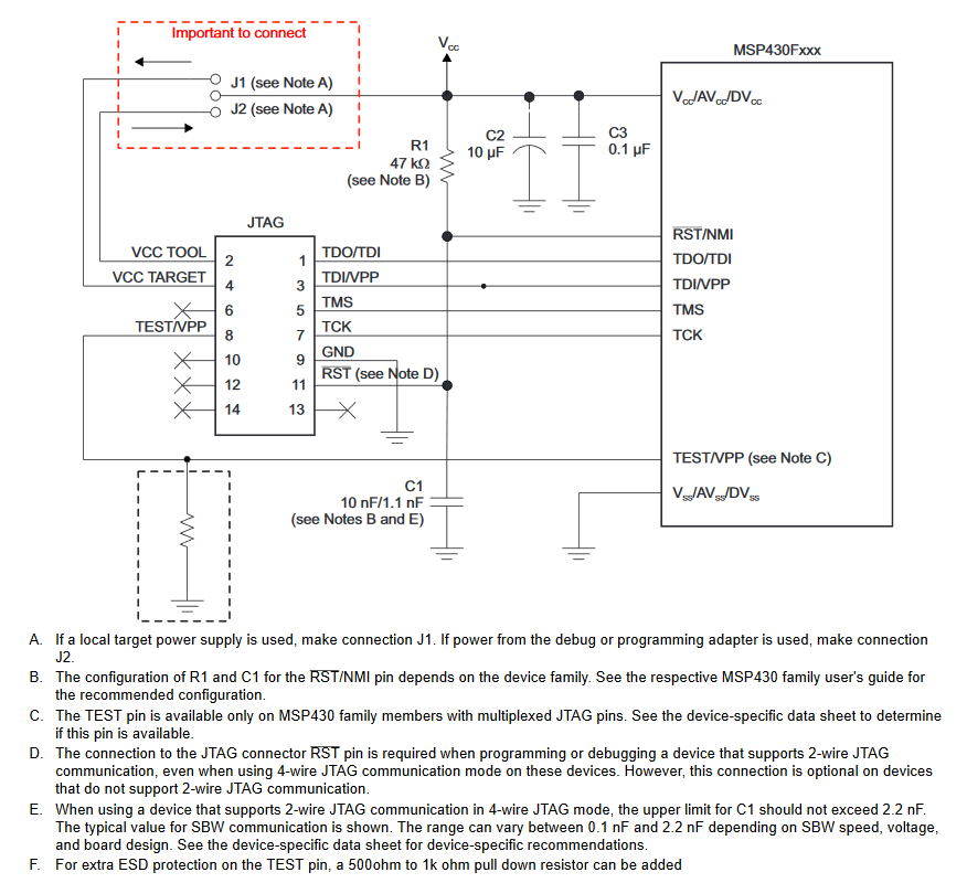
attached my schematics  for reference,

MSP430F2617TPM+DRV8886 Version1.pdf

Will you help to figure out why and how to fix those issues? thanks!

Regards

Lin 

  • Hi Li,

    Can you let me know the DVDD and AVDD abnormal voltage values?

    Let me research the issue with programming the MSP430 and I'll reply back with an answer by tomorrow.

  • Hi Pablo,

    Thanks for your kindly help.

    what I am talking about the abnormal voltage on pins of chip is DRV8886PWP.the detail value is as below:

    the DVDD pin when checked voltage is 1.5v; the AVDD pin  when checked voltage is 0v. 

    just a reminder.

    there are two issues for my understanding , one is the DRV8886PWP chip with certain problem cause  nFAULT pin keep logic low.

    another is the MSP430F2617 chip when download program, display hardware mismatch ,

    the step down voltage regulator output from LT3976 chip is 3.05v from this prototype PCB.

    Regards

    Lin

  • Hi Lin,

    Thank you for providing the information.

    A couple more questions for you:

    1. What is the VM voltage valuewhen fault occurs?
    2. Do you have a load being driven when the fault occurs? If so, can you provide a waveform of the load current when the fault occurs?
    3. When programming the MSP430, did you ensure to select the MSP430F2617 as the target device? from the error message, it looks like the MSP430F2618 is selected.
    4. The converter was programmed to 3.3V output correct? If the measurement is 3.05V, then there must be something pulling the voltage down.

    I checked your schematic and everything looks good. Have you checked the layout for any potential problems?

  • Hi Pablo,

    Thanks for your kindly help.

    from my prototype PCB, I provide the VM with value 24VDC there .

    I have chosen the msp430f2617 as target device already in IAR software  , previously  my  IAR software which have tested well when using DRV8886EVM board bought from Mouse. during then test , I had bypass the original GUI function, with enable/direction signal only for my test.

    I never had done any test  with a loading being driven.since above issues pending in this prototype PCB..this may cause driving not work at all.

    for 3.3V ,originally as purpose for my prototype , but when chose resistor not very suitable for voltage output value from step down regulator , which only control well at 3.05v , I think within TI msp specification and leave there. 

    for my PCB design file , I may provide files as a reference for your figure out  if possible.I also want to verify the layout for my PCB whether potential issue present or not , since I use EAGLE as PCB design platform,no enough experience there. .this reference is a Eagle project . 

    Regards

    LinBipolar Driver with MSP430F2617TPM.rar

    Regards

    Lin

  • Hi Lin,

    Thank you for providing the information. I am able to open the project files. let me take some time to review it and I will get back to you by tomorrow.

  • Hi Lin,

    I looked through the schematic and layout below are some of my concerns:

    In regards to the MCU programming. I did not see any obvious problem with the design that could be causing the issue. Most likely, the issue is on the IAR software. Can you try to program the same code with same IAR configuration on the DRV8886EVM. Is the hardware mismatch issue still present?

    Providing a procedure on how you program the board will also be helpful  to figure out what could be causing the issue. Can you provide the procedure.

  • Hi Pablo,

    Thanks for your advice.

    Regarding to the MCU programming; I have download successfully on DRV8886EVM with my program(just trigger enable_signal logic low  for my attached program ) ;no hardware mismatch issue .

    the procedure is following the msp430 Basics books provided procedure from which I learned.

    In option tab of IAR software,

    1  choose the right chip type in general options menu such as msp430f2617 as target device first,

    2  choose the right FET debugger as driver in debug menu;

    3  choose the right connection type in FET Debugger menu.

    4   press "make" button to make sure no errors ,if has , need revert to correct program.

    5     then press download and debug button .

    for nSLEEP and Enable pin, logically once program works; it may switch the logic accordingly to make the driver work when I tested with DRV886EVM.

    For the layout for MCU and DRV8886 on my PCB , certainly need be improved , but at least my strep down regulator still works for my layout, output 3.05v at least. so I am thinking why other two chips totally present  so abnormal issue? if your guys has more experience with  such issues for advise and learning , Do you may advise any problem for the  chips layout or why happened? if really no more figure out ,  I am trying to redesign this PCB with ultra librarian to make sure get the right component footprint for next trail test and meantime to watch your manual or videos for learning  the PCB layout for improving.IAR MSP430f2617_DRV8886_Stepper Driver.rar

    Regards

    Lin

  • Hi Lin,

    Thanks for providing the information.

    I am not too familiar with the IAR software myself but I will get someone else in my team to help out figure out what could be causing the programming error. It might take a couple of days until we figure out the issue. Expect a response by 1/12 or earlier.

    The MSP430 in your design has not been programmed. Is this correct? Just want to confirm.

    In regards to the PCB layout, I suggest doing the following improvements for the next board.

    • place the VM bulk capacitors (C3 and C20) closer to the driver
    • place thermal vias on the thermal pad of the driver IC
    • place C15 and C14 closer to the driver IC
    • Avoid having right angle traces like BOUT2 trace.
    • Place more GND vias on the board to connect the top and bottom layer GND planes.
    • route the signals such the amount of GND copper on both layers is maximized.

  • Hi Pablo,

    Thanks for your kindly figure out in detail for PCB improvement , I will do trying your suggestion when layout PCB later next time.

    For the IAR software support, thanks in advance as well for your sincere arrangement  for improvement  correction later by your team if possible.

    I am O.K. no need hurry for the answer. i just want to know which factors may cause likewise issues , any defects from my design fault  may cause that issue.

    I hope the function for DRV8886 driving chip may work  as the  original DRV8886EVM board tested as the video attached, looked pretty well for my feeling when I chose this chip .and since MSP430F2617TPM chip has DAC module so may  better fine tune the motion smoothly.; except the interface has to be modified by my application environment.  

    Let me say great  appreciation for your help.

    Regards

    Lin

  • Hi Pablo,

    Correct, the issue pending during download my program, thus I think my design has not been programmed successfully. after fix that issue, if program may step by step execute in IAR software platform, then I believe it means program works at least in right/matching memory location.

    Regards

    Lin

  • Hi Lin,

    Thank you for sharing the video.

    I think the first thing we need to figure out is what is causing the programming issue. Once the MCU is programmed correctly, then we can see if the nFAULT and the AVDD/DVDD issues are still present.

    I will give you an update by tomorrow.

  • Hi Lin,

    Did you populate J5 and let JP6 open? The schematic below shows the proper way of setting up the signal connections for 4-wire JTAG communication. A you can see R7 (in your schematic) should be connected to AVCC of the MCU for proper communication. I also suggest using the recommended values for capacitor and resistors.

  • Hi Pablo,

    Thanks for your  detail support set up  information for JTAG communication  area, 

    yes , I have  populated J5 and let JP6 open from my schematic.compared your provided schematics, the obvious difference is the R1/C1 values .and TEST pin not connected yet.

    but I reason differently  during analysis as below:

    I wonder I already follow the JTAG communication set up benchmark used on DRV8886EVM ; you may confirm my eagle files last sent. so if I change only the power supply from original FTDI regulator to LT3976 step down regulator, then original DRV8886 EVM set up JTAG sample  not work and need change as the way you present? whether not reasonable?

    anyway  I may verify  all of suggestion   once I  get another improved PCB ,but need time to work out.

    appreciate your advice and hope to  check and try once more. 

    Regards

    Lin

  • Hi Pablo,

    I verified the download message again for this prototype PCB   this afternoon , please see attached. you may see VCC voltage displayed at 1.2V, abnormal ? still detect the device as MSP430F2416 not original MSP430F2617TPM chip which I  ordered from TI .

    I also double confirm the voltage with multimeter on hand for  all PIns of JTAG port.

    these are as below:

    Pin1: 1.495VDC

    Pin3  3.32VDC DRV8886 Project IAR Message Display.pdf

    pin5: 3.32VDC

    Pin7:3.32VDC

    pin9  0VDC

    Pin11:3.34VDC

    Pin4: 3.35VDC.

    Maybe the VCC voltage displayed in IAR software too lower?

    Any abnormal finding from IAR software detected in this message?

    Regards

    Lin 

  • Hi Lin,

    This is interesting. Can you repeat the experiment above and measure all the pins of the JTAG pins of the DRV8886EVM.

    Give me a day to look at the IAR error message to see if it gives any clues as to what is happening. What I want to understand is why the IAR is detecting an MSP430F2416 and not the MSP430F2417.

  • Hi Pablo,

    The DRV8886EVM not on hand anymore now since I removing quite a lot of components form them during retrofit this  prototype PCB , to verify the size of  footprint of my PCB.

    Will you help to verify these signals on your side since current situation on my side, thanks so much if possible.

    no need hurry to get a result, you may check the clue from IAR software message in your pace.

    By the way ,just a reminder. The IAR is detecting an MSP430F2617 chip as an MSP430F2416 through my prototype PCB from  the error message.

    Regards

    Lin 

  • Hi Lin,

    Understood.

    I will work on understanding the JTAG signals from your prototype PCB first and try to understand why the IAR is misidentifying the MCU. 

    I can grab a DRV8886EVM from our lab to compare the JTAG signals if needed.

    Expect to hear back from me by the end of this week.

  • Hi Lin,

    The DC voltage values of the JATG won't give much information. Does this issue happen in multiple boards? or do you only have one prototype board?

    Unfortunately, I don't have the IAR software so I can't reproduce the issue on my side. There is another solution you can try. You can download UniFlash, free FLASH programmer utility from TI at https://www.ti.com/tool/UNIFLASH?keyMatch=UNIFLASH%20DOWNLOAD&tisearch=Search-EN-everything. This utility will allow you to program the MSP430 device using .out or .txt file generated with IAR or CCS, using the MSP-FET via the JTAG port, this would be a good cross check. It automatically detects the correct MSP430 device and displays it like so:

    Can you try this method and see if it works?

  • Hi Pablo,

    Yes, I have only one prototype PCB , this issue happened on this PCB  only.

    This PCB should have serious problem , whether I use IAR or CCS  when download program same problem happened , so even you proposed method still same: no device detected , let me dig more for a while .to verify every single pin whether at right position for my PCB first , once I get certain clue or finding , I will feedback what I observe incorrect point, thanks a lot  for your all kinds of suggestion .

    Regards

    Lin   

  • Hi Lin,

    Sounds good!

    Let me know about your findings and if you require further assistance.

    If you don't require further assistance at the moment, please click on "resolve" to close this thread. You can still reply to this post or ask a new related question if you require assistance in the future.

  • Hi Pablo,

    Appreciate for your so detailed help for all those areas before. hope when next prototype PCB made. this issue has gone away.

    Regards

    Lin