This thread has been locked.

If you have a related question, please click the "Ask a related question" button in the top right corner. The newly created question will be automatically linked to this question.

DRV8847: I2C Communication not working

Part Number: DRV8847

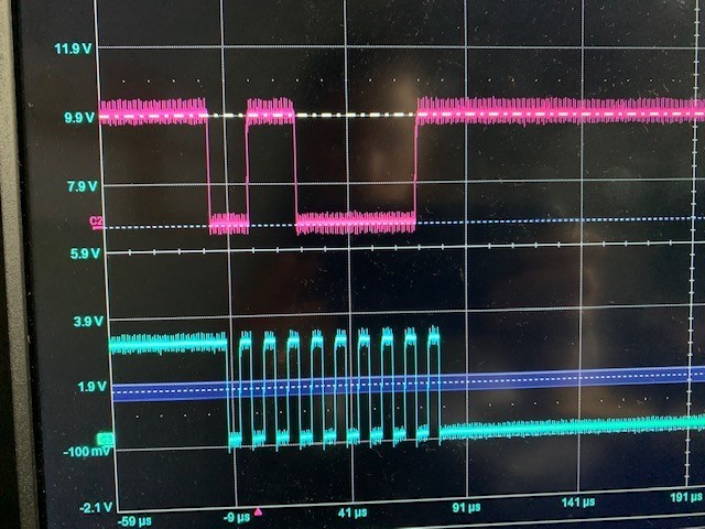
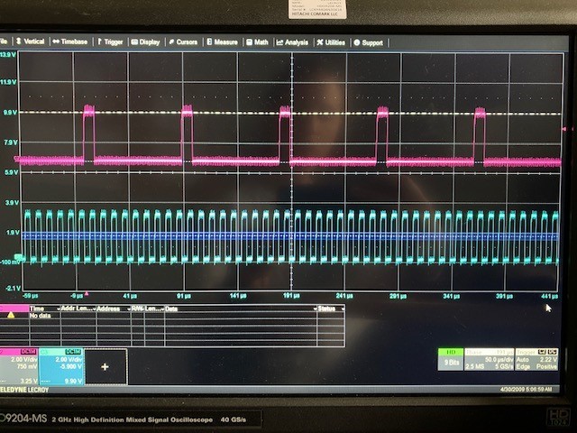
I'm having a very strange issue with the DRV8847S on a custom board.  I am using 3 of these parts on my board and therefore have to set the addresses for each. When I first write to address 0x60 (the default address), I never get an ack as shown in the first picture below and the clock stays low.  After a short bit of time (< 1 second), the bus gets stuck in the mode shown in the second picture.  I can't for the life of me figure out why.  Also, when I write to another device on the bus, the bus gets "unstuck" and writes/reads successfully. Can anyone provide some insight?


  • Katrina,

    Are you following the steps outlined below in the datasheet:

    The DRV8847S device variant is configured for multi-slave operation by writing the DISFLT bit (IC2_CON register) of all connected devices to 1b. This step will disable the nFAULT output pin of all DRV8847S, to avoid any race condition between master and slave I 2C device.

    • Pull the nFAULT pins (nFAULT2, nFAULT3, and nFAULT4 pins) of three devices (2, 3, and 4) to low to release the I 2C buses of the slave device (device-2, device-3 and device-4). Now only device-1 is connected to master.

    • Since, only one device, DRV8847S (1), is connected to the controller, and, therefore, its slave address can be reprogrammed from default 0x60 (7-bit address) to another unique address.

    • Similarly, the slave address (SLAVE_ADDR) of the other three devices (device-2, device-3 and device-4) can be reprogrammed sequentially to unique addresses by a combination of nFAULT pins.

    • When all slave addresses are reprogrammed, write the DISFLT bit to 0b (IC2_CON register). This will enable the nFAULT output pin for fault flagging.

    • All the nFAULT pins are released and a multi-slave setup is complete. Now all connected slave devices can be accessed using the newly reprogrammed address.

    • The above steps should be repeated for any device in case of a power reset (nSLEEP). .

    From the scope capture, it looks like you are doing a READ.  For a WRITE, the last bit after the address should be 0.  

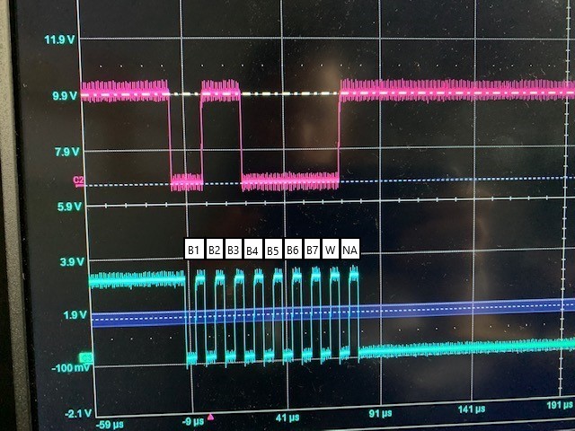
  • I am aware of what the datasheet says is required in order to allow multiple DRV8847S devices on one bus.  My problem is that I can't write to it, period.  Also, if you look at the labeled image below, you can see the address is B1-B7, the read/write bit is indeed a 0 for a write (W) and the last clock pulse is supposed to allow for the device to ACK the communication by keeping the data line low--this is what is not happening (NA=Nack).

  • Katrina,

    Is the transmitter releasing the bus after sending the last "W" bit?  

    https://www.ti.com/lit/an/slva704/slva704.pdf

    See section 2.3 of the app note linked above.  

  • Yes--I use the same software function for this part as I do for other parts on the bus.  I am successfully able to write to and read from every other device except for this one.

  • Ok, let me dig around for another possible explanation.

  • Few more questions to help debug:

    1)  Are you pulling the nFAULT pins (nFAULT2, nFAULT3 pins) of the other 2 three devices (2, 3) to low to release the I 2C buses of the slave device (device-2, device-3). Now only device-1 is connected to master?

    2)  If this doesn't work, try putting the other 2 devices in the sleep state by holding nSLEEP pin low.  

  • I pulled the nFault of two out of three of the devices low after attempting to write to the IC2_CON register to disable the nFault capability--this didn't work because I couldn't successfully write to the IC2_CON register.  I have not tried to sleep the other two devices--that is a great idea to try.  I will get back to you after I try that tomorrow.  Thanks!

  • Katrina,

    Thank you...look forward to the results.

  • I am still having the same problem.  I have a question though--how exactly does the nFault pin interact with the I2C bus?  For example, if I didn't write to the register to disable the nFault functionality, but I was pulling nFault low unintentionally, what would happen?  Would the I2C bus not work?  Currently, the nFault pin is low, but I have nothing connected to the output, so I would expect the OLD detection feature to pull that pin low. My goal is to just get the device to ACK the starting address of 0x60.  Then I can take it from there, but I don't understand why it's not generating an ACK.  The oscope waveform looks good and I measured the I2C bus right on both the SDA and SCL pins to verify it was getting to the IC. 

  • Very interesting observation.  When nFAUT is low, the device is released from the I2C bus. 

    From the datasheet:

    "Fault indication pin. This pin is pulled logic low with a fault condition. This open-drain output requires an external pullup resistor. This pin is also used as an input pin for the DRV8847S device for releasing the I2C bus"

    This is typically done externally with the MCU I/O operating as an output pin during the address reprogramming and then acting as an input to monitor the fault status.  

    Can you test the theory by connecting a load to avoid the OLD?  Power resistor or motor will do.  

  • I connected 2 power resistors to the output of one device, put the other 2 devices in sleep mode and made sure the one device I wanted to talk to was not faulted and not in sleep mode (I measured the pins directly on all devices to determine this).  I also made sure the assembly house placed the correct part--the marking is 8847SPW, so it is correct.  I'm still running into the same issue--the oscope waveform looks exactly as in my original post.  I'm 100% sure the bus is working since I can successfully talk to every other device on the bus.  I am able to get the device to perform correctly using the discrete inputs, so I also know that the power is set up correctly.  Interestingly, in the block diagram in the datasheet for this part, I noticed that there is only an external pull up on the SDA line and it shows an internal pull down resistor on the SCL--is this accurate?  Per the I2C standard, there is supposed to be an external pull up on both lines (which I do have), but I'm curious about the internal pull down on the SCL line.

  • Let me pull in some more people on my end and see if they have any ideas.  

    On the EVM, we do have a 10k pull-up on each line...SDA and SCL.  I am not sure about the internal pull down, but it does not appear to be affecting the signal levels in a negative way.

  • A colleague took another look at the scope capture and it appears the address might be incorrect.  

    Bits 1-7 appear to be 0110000 = 0x30.  This should be 0x60 for the address...1100000.

    Or, if you include the R/W bit, the transmitted data should be 0xC0.  

    Can you please double check this?  

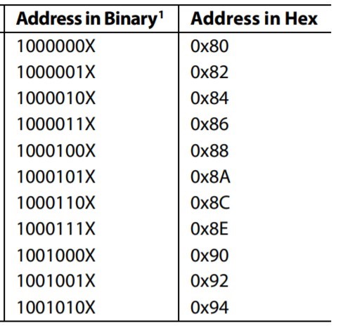
  • Yes that is it--most datasheets that I have seen state the address with the assumption that the read/write bit is a 0.  This datasheet was very confusing.  Maybe adding in the actual bits would be helpful?  I have attached an example below.  Thank you so much for your help.

  • Glad it is working and understand your point.  I had to think about it as well.  I will feedback to the development teams.

    Let me know if you have any more issues.