


Dear colleague,
Our customer had post this issue previously, but don't get the confirmed answer.
So I summrize the test progress and issue, customer just want we confirm whether their operation is reliable.
1. The timing of reading fault register:
1)The timing diagram of the data manual is: at the beginning, LATCH is high -> CLK is pulled low -> LATCH is pulled low -> LATCH is high -> CLK is high, then at CLK falling edge exchange data, then read data, and finally CLK is low -> LATCH is low. The fault register data we read according to this sequence is incorrect, similar to a left shift.

2)The timing of this part of the MSP430 evaluation board program provided by the official website is like this: the beginning is different from the data sheet, and the “LATCH_LOW“ is shielded at the end, which is also different from the datasheet. Differences have marked in red. We found that the fault register data read by the evaluation board and example code for the first time also has a left shift phenomenon, and the data read for the second time and later are correct.
case 0xa6: // read back fault register
//LATCH-CLK pattern to clear the false pushing of fault register
CLK_HIGH;
LATCH_HIGH;
Delay_us();
CLK_LOW;
Delay_us();
LATCH_LOW;
Delay_us();
CLK_HIGH;According to the datasheet, this sentence should be after LATCH is high, but the data cannot be read correctly after switching.
Delay_us();
LATCH_HIGH;
for(ir=1;ir<=8;ir++)
{
CLK_HIGH;
Delay_us();
CLK_LOW;
Delay_us();
(P3IN & BIT2)?( ReadBack_Fault[0] |= (1<<(8-ir)) ):( ReadBack_Fault[0] &= ~(1<<(8-ir)) );
}
for(ir=1;ir<=8;ir++)
{
CLK_HIGH;
Delay_us();
CLK_LOW;
Delay_us();
(P3IN & BIT2)?( ReadBack_Fault[1] |= (1<<(8-ir)) ):( ReadBack_Fault[1] &= ~(1<<(8-ir)) );
}
for(ir=1;ir<=8;ir++)
{
CLK_HIGH;
Delay_us();
CLK_LOW;
Delay_us();
(P3IN & BIT2)?( ReadBack_Fault[2] |= (1<<(8-ir)) ):( ReadBack_Fault[2] &= ~(1<<(8-ir)) );
}
for(ir=1;ir<=8;ir++)
{
CLK_HIGH;
Delay_us();
CLK_LOW;
Delay_us();
(P3IN & BIT2)?( ReadBack_Fault[3] |= (1<<(8-ir)) ):( ReadBack_Fault[3] &= ~(1<<(8-ir)) );
}
Delay_us();
//LATCH_LOW;According to the datasheet, it should be pulled down, but the data cannot be read correctly after being pulled down.
2. Assuming that the evaluation board example is correct, we continue to test and find that the fault register is cleared after resetting, and then the fault register data read for the first time also has a left shift phenomenon, and the second time and later data read is correct.
The following is the detailed test process:
1). Test conditions: OUT2 remains open.
2). Test method: first reset the fault register, delay 10ms, and then read the fault register twice continuously, and repeat the operation in this way.
3). Test phenomenon: After each reset of the fault register, the data of the fault register read for the first time is shifted, and the data read for the second time is correct.
4). The test procedure is roughly as follows:
while(1)
{
drv8860.stu_fault = DRV8860_ReadFault();
drv8860.stu_fault = DRV8860_ReadFault();
Delay_ms(10);
DRV8860_Write_Special_CMD(1,2,4,3);//DRV8860_RESET_FAULT
Delay_ms(10);
}
uint16 DRV8860_ReadFault()
{
uint16 dat=0;
uint8 i;
CLK_H();
LATCH_H();
CLK_L();
LATCH_L();
CLK_H();
LATCH_H();
for (i = 0; i < 8; i++)
{
CLK_H();
CLK_L();
dat <<= 1;
if (DOUT_PIN) dat |= 1;
}
for (i = 0; i < 8; i++)
{
CLK_H();
CLK_L();
dat <<= 1;
if (DOUT_PIN) dat |= 1;
}
DRV8860_Delay();
//LATCH_L();
return dat;
}
void DRV8860_Write_Special_CMD(uint8 part1, uint8 part2, uint8 part3, uint8 part4)
{
uint8 i;
LATCH_H();
CLK_L();
LATCH_L();
for (i = 0; i < part1; i++)
{
CLK_H();
CLK_L();
}
LATCH_H();
LATCH_L();
for (i = 0; i < part2; i++)
{
CLK_H();
CLK_L();
}
LATCH_H();
LATCH_L();
for (i = 0; i < part3; i++)
{
CLK_H();
CLK_L();
}
LATCH_H();
LATCH_L();
for (i = 0; i < part4; i++)
{
CLK_H();
CLK_L();
}
LATCH_H();
}
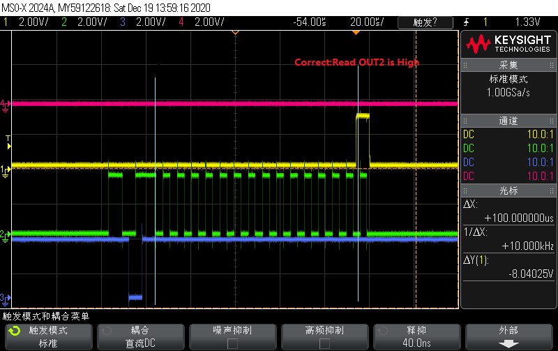
The following is the first reading of the wrong data waveform:
Yellow color: DOUT
Green color: CLK
Blue color: LATCH
Red color: DIN

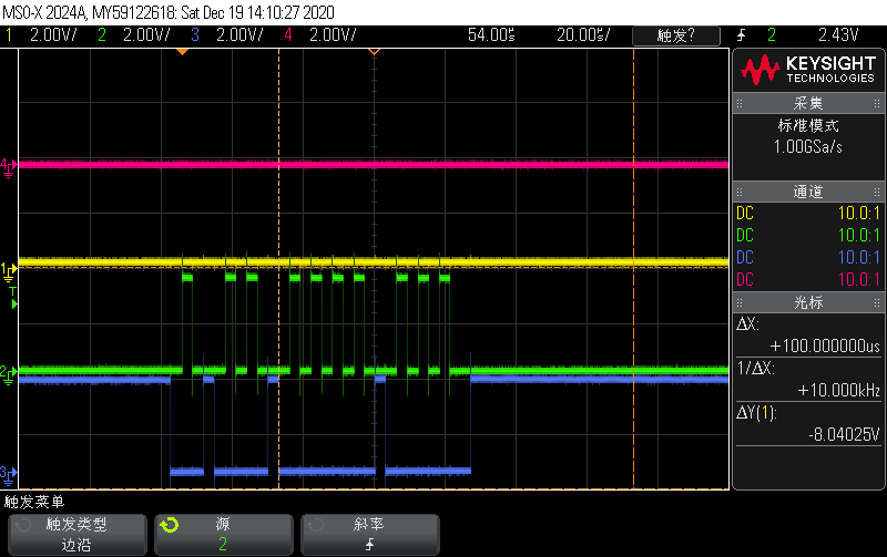
The following is the correct data waveform read for the second time:
The following is the waveform of the reset fault register:
3.Continuing the test, we found that the additional CLK high and CLK low are added at the beginning of the timing of reading the fault register. Then the data read for the first time or the second time is correct, but there is no reliable basis, please confirm it.
uint16 DRV8860_ReadFault()
{
uint16 dat=0;
uint8 i;
CLK_H();
CLK_L();
CLK_H();
LATCH_H();
CLK_L();
LATCH_L();
CLK_H();
LATCH_H();
Best Regards,
Rock Su

