This thread has been locked.

If you have a related question, please click the "Ask a related question" button in the top right corner. The newly created question will be automatically linked to this question.

DRV8353: VM/VDRAIN Connection

Part Number: DRV8353
Other Parts Discussed in Thread: DRV8350

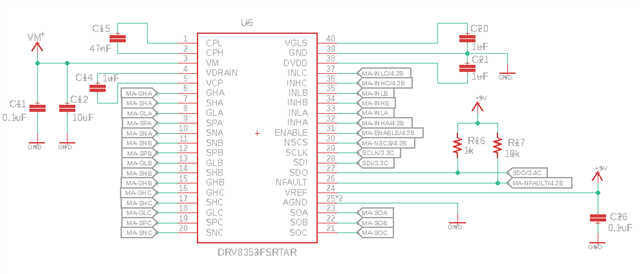
Figure 9-1 of the DRV8353 datasheet shows a direct connection between VM and VDRAIN. This connection is not indicated on figure 8-1 through 8.8. It is also not shown of the schematic for the DRV8353 EVM. Is the connection shown on 9-1 correct?

  • Rodney,

    Thanks for posting on the MD forum!

    I am not seeing the figure numbers you are mentioning, probably just a formatting difference. Regardless I can explain:

    In a nutshell, VM and VDRAIN can be a shared connection if the motor is to be driven by the same supply as the DRV is using. To save power, the VM connection can be split from the VDRAIN connection so that the DRV is powered from lower voltage while the VDRAIN pin is still used by the charge pump to reference the motor voltage which is higher.

    "The gate drivers can operate in either a single or dual supply architecture. In the single supply architecture, VM can be tied to VDRAIN and is regulated to the correct supply voltages internally. In the dual supply architecture, VM can be connected to a lower voltage supply from a more efficient switching regulator to improve the device efficiency. VDRAIN stays connected to the external MOSFETs to set the correct charge pump and overcurrent monitor reference."

    Regards,

    -Adam

  • To add on to Adam's point, we have an app note describing the difference between single supply and split supply operation when using the DRV8350: LINK

    Thanks,

    Matt

  • Thank you both for responding. I am about to finalize a design using the DRV8353. I have included the schematic. VM is 48 vdc. The drains for all 3 high side MOSFETs are also tied to VM. Would you mind telling me if it will or will not work or maybe suggest an improvement? I do have a regulated supply to 12v on the same board if it makes more sense to use that to supply VM on the driver.

  • Hi Rodney,

    Using a lower voltage on VM is preferred to reduce the power dissipation.

    Schematic comments:

    1) C20 should be rated 25V

    2) C15 should be rated 100V (same as C16)

    3) C16 (and other similar bypass capacitors) can be more useful when they connect to the top of the sense resistor (low-side MOSFET source). This helps mitigate inductance in the sense resistor and in the ground path on the board.

    4) Having a footprint for a snubber across each MOSFET may help int he future if you run into parasitic inductance issues. These MOSFETs are leaded packages so they do have a significant amount of inductance.

    Thanks,

    Matt

  • Hi Rodney,

    Schottky diodes are only rated 40V, should be at least 60V like mosfets.

    Regards,

    Grzegorz 

  • Grzegorz - thanks for pointing that out as well.

    Thanks,

    Matt

  • Hi,

    One more thing. There is a chance of getting problems withs dv/dt shoot through using these Mosfets.

    I would look for mosfets with better Cgd/Cgs (smaller) ratio and Qgd<Qgs.

    Regards,

    Grzegorz