This thread has been locked.

If you have a related question, please click the "Ask a related question" button in the top right corner. The newly created question will be automatically linked to this question.

DRV8353: Short circuit

Part Number: DRV8353

Hi Team,

The customer is experiencing below issue and needs your help.

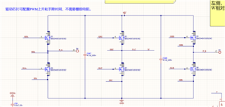
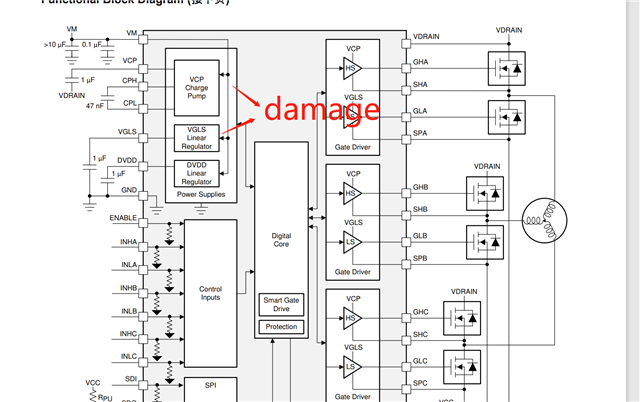
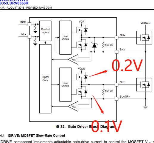
1. During the initial configuration of the chip, IDRVIEP=1A, IDRVIEN=2A. MOS is BSC040N10NS5, Qgd=12~18NC, it often happens that the totem pole circuit inside the driver chip is damaged. For example, the voltage value of the diode between VGLS and GLX is only 0.1V (normally measured near 0.59V). The voltage value between VCP and GHX is only 0.2V. After the fault occurs, the drive chip reports an undervoltage fault, and the VGLS and VCP voltages are insufficient. The customer suspected a short circuit inside the chip, and the temperature quickly rose to the alarm value after power-on.

2. After the customer reduces the drive current (IDRVIEP=0.1A, IDRVIEN=0.2A), VGLS and DVDD cannot output 11V and 5V during operation. There is a short circuit inside the chip, and the chip temperature rises sharply.

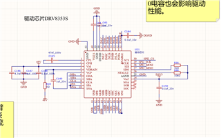
3. In the chip manual, DVDD is a 5V power supply. If it is not used, can the 1uf filter capacitor be removed?

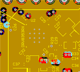
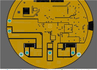
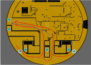
4. Whether the VDRAIN of the chip must be connected to the drain of the upper bridge arm of the MOS during PCB layout? What impact will VM and VDRAIN have in the design process? Will it cause chip damage?

Thanks.

Annie

  • 48V input, drive current is 100mA and 200mA. In the open-loop control motor running state, when vq is greater than 2V, the drive chip will report an error: Undervoltage and overtemperature. Then the current flowing through the driver chip increases sharply, and there should be a short circuit inside the driver chip. After power-on, it is found that VGLS and DVDD have no output. 

    8 chips have been broken.

    The driving waveform VGS of the upper and lower bridge arms is normal. Dead zone is also 400ns. The figure below is the schematic

    Thanks,

    Annie

  • Hi Annie,

    Thank you for your question!

    1. Has the customer tried using a brand new driver starting with 100mA/200mA IDRIVE settings, or has the customer always started out operating with the 1A/2A setting before changing it to the lower setting? Based on the Qgd of the MOSFETs they are using it may be the case that the 100mA/200mA IDRIVE setting may still be too high for their design. If the Qgd was on the lower end  ~12nC, this would result in a turn on time as fast as 12nC/100mA = 120nS, and a turn off time as fast as 12nC/200mA = 60nS which is quite fast for most designs and could cause damage to the driver. Most customers consider a turn on/turn off time of 200nS/100nS as a fast turn on time. We also recommend a minimum trace width of 20mils for the gate traces to help reduce the inductance of the path. Higher inductance on the gate trace results in increased ringing on the gate/source of the MOSFETs and causes the MOSFET to not be able to handle as high of an IDRIVE. If the IDRIVE is too high this can result in excessive ringing on the gate/ source and can damage the driver. They may consider starting out with the lowest IDRIVE setting (50mA/100mA).  

    2. Has the customer only tried this IDRIVE setting after operating the drivers at the highest IDRIVE setting? Since 1A/2A is extremely high IDRIVE for the customer's MOSFETs I would expect as you mentioned this could be the result of a short in the driver due to ringing on the gate/source of the MOSFETs resulting in damage to the driver. As mentioned before, 100mA/200mA  still might be too high for the MOSFETs, and thus could be a possible reason for damaging the driver, though it isn't as likely as operating it at the 1A/2A setting.

    3. Even if the DVDD pin is not used to power any external circuitry, it is still important to keep the DVDD capacitor since there is internal circuitry in the driver that is powered by the DVDD voltage.

    4. VDRAIN should be supplied from near the drain of the high side MOSFET if possible, since the voltage at VDRAIN is used to determine the drain voltage of the MOSFETs as well as supply the charge pump voltage. If VDRAIN is supplied close to the high side drain then the DRV drain voltage reading will be more accurate. VM is the voltage that is used to power the device, which can be the same voltage as VDRAIN, or a lower voltage can be used if desired.

    How long does the device operate before the device gets damaged? Is it immediate or does it operate for a short period of time before getting damaged?

    I am a little confused about what you mean by Vq, would you be able to elaborate more on what you mean by Vq?

    I have included an article on best practices for motor driver layouts that might be helpful, as well as an FAQ about selecting IDRIVE

    https://www.ti.com/lit/an/slva959a/slva959a.pdf

    (+) [FAQ] Selecting the Best IDRIVE setting and Why this is Essential - Motor drivers forum - Motor drivers - TI E2E support forums

    Regards,

    Anthony 

  • Hi, Anthony

    Thank you for you answer!

    I have some new questions after testing.

    During the test of the quick start, there will be a current surge that cause instantaneous damage to the drive.

    my motor drive input voltage is 48V, VM and VDRAIN  are connected together on the PCB, both connected to 48V.

    1、In the fast start state, a large current surge will cause internal damage to the driver chip. After testing, We found  VGLS cannot output 14.5V , and the VGLS output becomes a pulse wave. The maximum value of the pulse is about 3V, the minimum value is 0V. meanwhile, the internal loss of the driver chip about 4W. it seems that the VGLS Linear Regulator is damaged. there is a short circuit inside the driver chip.

    2、After the fault occurs, the VCP output is 48V, but the normal state is 58V. the CPH voltage is constant at 48V, the CPL voltage is constant at 0V, and the fault feedback is UVLO, OTSD and GDUV.

    3、The impedance of VGLS to ground is normally 1M, and it is about 2.2K after damage. DVDD output 5V is normal.

    4、After the fault occurs, sometimes the A-phase lower arm push-pull circuit is damaged. The diode voltage of VGLS and GLX is only 0.1V, and there is a short circuit between GLX and SLX.   MotorDrive_PCB.PcbDoc

    This is PCB design, If the design is unreasonable, please give some suggestions, thank you.

     I hope to get your suggestions

  • Hi Yao,

    I agree with your analysis that it seems like the driver is getting damaged resulting in an internal short. In the fast start state, what is your IDRIVE setting that you are using? What method of commutation are you using? (trapezoidal, sinusoidal, or FOC)? Does your system have hall sensors? Or is it sensorless? You mentioned that there is a short circuit between GLx and SLx. Is this on all the phases or just on one phase? 

    I looked at the layout and have a few observations.

    1. The gate traces are a little thinner (13mil) than would be desired (20mil). You can widen the traces once you are far enough away from the device so that you have sufficient room. This will help reduce the inductance of the gate traces and will help reduce ringing of the gates.

    2. For phase B, I noticed that the traces have to go through vias to go underneath phase C. This will increase the inductance of those traces, so you may see more ringing on this phase compared to the others. Due to this, it is especially important to have wide gate traces for that path.

    3. I would recommend looking to see if you can move the capacitors surrounding the device as close as possible to the device, prioritizing the CPH-CPL capacitor and the VCP-VDRAIN capacitor  

    4. I noticed you have a 100pF capacitor between the Gx and Sx pins of the MOSFETs. What goal are you trying to achieve by adding this additional capacitance? 

    In your design, it looks like the motor connects right at the center of the switching node. I would recommend seeing if it is possible to offset the motor connections so that they are not directly in line with the switching node. If the motor connects right at the center of the phase node this can introduce ringing at this point, however if the motor connection is offset from the phase node than that may help reduce ringing.  If you notice in the image below (which is an example MOSFET configuration in our Best Practices for Motor Driver Layouts app note) , the motor connection is off to the side (circled in red), whereas your design has the motor connection in the center of the phase node (where the blue arrow is pointing). 

    I noticed you are using the DRV8353S but aren't using the current sense amplifiers. If you do not plan on using sense resistors on the phases than you could consider switching to the DRV8350S. The DRV8350S is similar to the DRV8353S except it doesn't have the current sense amplifiers. 

    Regards,

    Anthony 

  • Hi, Anthony

    Thank you for you answer! Sorry to reply you so late.

    The config registers are the following:

    Reg 0x02 = 0x4AI           0100 1010 0001

    Reg 0x03 = 0x311           0011 0001 0001

    Reg 0x04 = 0x711           0111 0001 0001

    Reg 0x05 = 0x36B          0011 0110 1011

    Reg 0x06 = 0x382           0011 1000 0010

    So, IDRIVEP setting 50 MA, IDRIVEP setting 100 MA. The control method is FOC, and we use magnetic position sensors to collect location data. The short circuit between GLx and SLx only occurs in phase A.

     the 100pF capacitor between the Gx and Sx pins of the MOSFETs is reserved debugging pad, I plan to connect 10K resistor between the Gx and Sx pins to absorb the CGD impulse voltage.

    In next design, I will adopt your layout opinion.

    Now, I have some new questions。

    1、 the capacitance of VGLS to ground is EDK063BBJ105MPLF (0201 16V). Is the VGLS capacitor voltage rating too low?

    2、Does the ground of the driver chip need to be connected to the power ground at a single point?As shown in pcb picture, The driver groung GND_DRV is connected to Power   
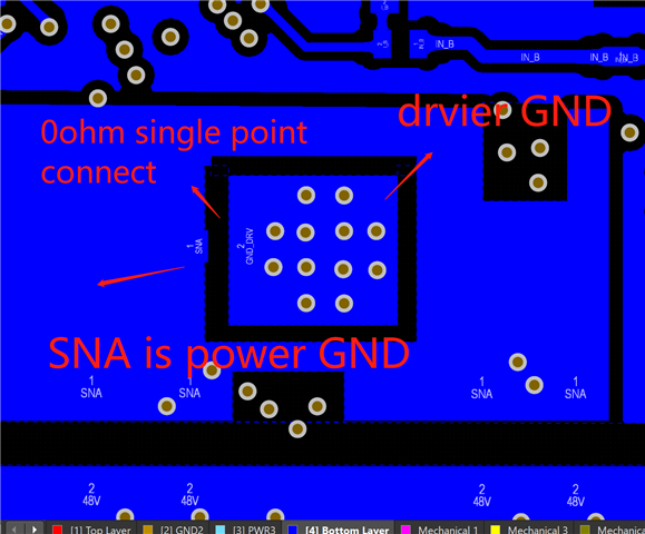
GND through a 0 ohm resistor

    3、What is the driving signal line(GHX, SHX,GLX,SLX) distance setting, and whether 7-8mil is too small?

     I hope to get your suggestions.

    Regards

    Yao

  • Hi Yao,

    1. A 16V capacitor for VGLS is quite low since the VGLS typical voltage (when VM = 15V) is 14.5V and the max voltage with the same VM is 16V. it is good to have 2x margin for the voltage rating of the cap if possible. Although the datasheet recommends a 16V cap I would recommend using a 25V or 35V cap due to derating and voltage transients.

    2. The grounding scheme that you are using here will create issues due to the restriction of current flow returning back to the system ground. Most of the heat dissipation is supposed to be through the thermal pad of the DRV to the copper pour that is connected directly to the pad. but in your case all the current has to flow through the 0 ohm resistor which is not ideal. For our EVM (shown below) you can see how current can flow out of the thermal pads in all directions. In this case our EVM doesn't have a split ground scheme, but the principle is still the same: it is best to connect the ground pad to a large copper pour with a short return path back to ground. 

     I would recommend the following changes:

    a. Figure 1 is your current ground scheme, which has the thermal pad as an island with all the current from the DRV having to go through the 0 ohm resistor. In figure 2 I have connected the DRV ground to the main ground on two sides to allow for more current flow from the DRV straight back to the system ground. This will also result in better thermal performance since the heat is not concentrated on the thermal pad since I have attached it to a larger copper area. in figure 2, The red arrows shows the path of the current flow from the MOSFETs back to ground, and the blue arrow shows the path of the current flow from the DRV back to the ground. 

    figure 1

    figure 2

    b. I would try to increase the area of the copper connected directly to the thermal pad as much as possible, since this will improve thermal performance. 

    c. For the D3V3 external bypass capacitor I would recommend attaching it to the DRV ground instead of DGND. 

    d. I couldn't figure out where DGND is connected to the system ground in the layout. Make sure that DGND has a good return path to the system ground and is connected appropriately to reduce any differences in the ground potentials. 

    3. the minimum distance between two traces such as the GHx, and SHx or GLx and SLx will vary depending on the PCB manufacturers' minimum trace-to-trace distance. I would recommend not routing the GHx and GLx traces next to each other (which it looks like that isn't a problem in your layout), since doing so could result in parasitic capacitance between the high and low side gates that could result in coupling issues with the switching of the gates.

    Implementing these changes should go a long way in improving your design.

    Regards,

    Anthony