This thread has been locked.

If you have a related question, please click the "Ask a related question" button in the top right corner. The newly created question will be automatically linked to this question.

DRV8353R: Gate Driver problem

Part Number: DRV8353R
Other Parts Discussed in Thread: DRV8353, DRV8323

Hi,

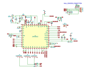
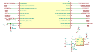
I'm using DRV8353RHRGZR for our motor control application and stuck at final proto testing.

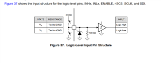
using it in 1 x PWM Mode, many time's their is 800mV on(INHA pin)PWM input pin which is connected to MCU and (INHC pin) Direction pin which is pull down by 10K resistor,

Due to the voltage on the PWM pin((INHC) the gate driver consider it as 100% duty cycle and then all goes wrong, I've replace the IC but still their is voltage on both the pin's.

My observation: whenever  I change the direction of the motor by using the Direction pin ((INHC) from that instant their is voltage on the that PIN

  • Thank you for your question!

    Would you be able to provide your schematic showing the MCU connections to the INHA and INHC pins along with any external components attached to these pins? When you change the direction of the motor using the Direction pin is this done while the motor is spinning? Or do you break and stop the motor first and then change directions? What is the reason you chose to use an external 10K pulldown resistor on the INHC pin? The INHx pins have an internal pulldown resistor of 100k ohms (see picture below)

    You mention that once this condition happens where you see the 800mV on the pins, all goes wrong. What exactly goes wrong? Is there sudden speedup of the motor? is there any faults? Does the motor stop spinning? 

    Regards,

    Anthony 

  • Hi Anthony,

    I have tried one more time after post my query, by replacing the Gate driver IC it works one day perfectly. but now the gate driver goes in fault whenever I start the motor, I've check that two pin(INHC & INHA )  and know their is near about 1.2V on that pin, I've also check the Resistance of that two pin with respective ground of DRV8353 and it shows 8.2K,

    The direction is change only at the power up not at a time when motor is running,

  • Hi Chaitanya,

    I have a few more questions for you:

    1. You mentioned that there is 1.2V on the INHC and INHA pins that you have measured. For the INx pins a voltage is considered high if it is between 1.5V and 5.5V, it is considered low if it is between 0V and 0.8V. So 1.2V is not desirable to have on an input pin since this voltage is neither a high signal or a low signal. Are you measuring this while applying a 3.3V signal from the MCU? 

    2. What is the resistance of the INHC pin when you remove the 10k resistor?

    3. Would you be able to provide me with the part number for the MCU?

    4. It looks like you are using 2 different grounds for the MCU and DRV. If so, would you be able to probe those 2 ground points to see if they are at a different voltage potential? Also I don't see any place on the schematic where the DRV ground and the MCU ground are connected together. Are they connected together on the layout? 

    5. Do you only notice issues when the direction pin is set to a certain direction? Example: INHC pin is low, does not operate normally. INHC pin is high, operates normally. 

    6. Do you see the motor start to spin at all prior to the fault occurring at startup?

    Regards,

    Anthony 

  • 1. You mentioned that there is 1.2V on the INHC and INHA pins that you have measured. For the INx pins a voltage is considered high if it is between 1.5V and 5.5V, it is considered low if it is between 0V and 0.8V. So 1.2V is not desirable to have on an input pin since this voltage is neither a high signal or a low signal. Are you measuring this while applying a 3.3V signal from the MCU? 

    I'm measuring after applying  5v to the enable pin of DRV8323

    2. What is the resistance of the INHC pin when you remove the 10k resistor?

    67.8K

    3. Would you be able to provide me with the part number for the MCU?

    4. It looks like you are using 2 different grounds for the MCU and DRV. If so, would you be able to probe those 2 ground points to see if they are at a different voltage potential? Also I don't see any place on the schematic where the DRV ground and the MCU ground are connected together. Are they connected together on the layout? 

    i have probe the two ground and their is no potential difference between them i have short this ground by 0R on layout,

    5. Do you only notice issues when the direction pin is set to a certain direction? Example: INHC pin is low, does not operate normally. INHC pin is high, operates normally. 

    initially its work fine but (first time with new IC) but after few cycle the pin float to some voltage

    INHC pin is low, does not operate normally. INHC pin is high, operates normally.  this also  happen several time

    I'm enable to predict the behavior of DRV will you please help me to protect the DRV from getting Damage

    IDrive 75K to VDD(450mA), i have also provide the external gate resistor for limiting the gate curret

    most of the time only C phase of driver get damage(gate to ground resistance less than 1K)

    6. Do you see the motor start to spin at all prior to the fault occurring at startup?

    yes it try to rotate, I think its because of IDrive fault

  • Hi,

    will you please give me little bit more information related to Mosfet support by this gate driver

    from datasheet:

    The DRV835x family of devices MOSFET support is based on the MOSFET gate charge, VCP charge-pump capacity, VGLS regulator capacity, and output PWM switching frequency. For a quick calculation of MOSFET driving capacity, use Equation 11 and Equation 12 for three phase BLDC motor applications.

    Trapezoidal 120° Commutation: IVCP/VGLS > Qg × ƒPWM

    (I'm using internal charge pump voltage for the gate driver i.e VM pin connected to VBatt,

    so IVCP =25mA, VGLS= 15V ,

    IVCP/VGLS=1.66 e-3

    what happen if this is

    1.exactly equal to the Qg x ƒPWM

    2. Qg x ƒPWM is greater than IVCP/VGLS

  • Awaiting for your Valuable Reply

  • Hi Chaitanya,

    DRV8353 is a quite popular driver and quite a lot of designers have problems with them. I would start from analysis a few similar cases from links below.

    https://e2e.ti.com/support/motor-drivers-group/motor-drivers/tags/DRV8353

    e2e.ti.com/.../DRV8353R

    Damage to this kind of drivers is usually caused by ringing, overshoot and undershoot of voltages in Mosfet circuit. That is causing violation of Maximum Absolute Rating and damage to driver IC. Analysis of diagram, pcb layout, driver settings and oscilloscope measurements are needed to resolve such problems.

    Regards,

    Grzegorz

  • thanks Grzegorz,

    will you plaese help me to understand the following

    Trapezoidal 120° Commutation: IVCP/VGLS > Qg × ƒPWM

    (I'm using internal charge pump voltage for the gate driver i.e VM pin connected to VBatt,)

    so, IVCP =25mA, VGLS= 15.22V (this is the voltage which I've measure across the VGLS with resp to GND) ,is it correct ?

    IVCP/VGLS=1.66 e-3

    so,if I want to keep my switching freq 20Khz then my MosFet gate charge must be less than 83nC

    what happen if this is

    1.exactly equal to the Qg x ƒPWM

    2. Qg x ƒPWM is greater than IVCP/VGLS, does this damage gate driver

  • Hi Chaitanya,

    There are two auxiliary supplies in DRV8353, one for HS gate drivers and another one for LS gate drivers. Each of them has 25mA capacity. I guess for trapezoidal commutation only one Mosfet per side (LS or HS) is being turned on per PWM cycle, so you have first equation No 11. I think the maximum Qg of Mosfet in that case will be

    Qgmax = 0,025A/20000Hz = 1,25 uC. - you can compare it with equation No 33.

    I think 1250 nC is quite a lot for power mosfet and you should not worry unless you intend to use really big mosfet (or a few in parallel) plus higher switching frequency.

    Regards,

    Grzegorz

  • Hi Chaitanya,

    The I_VCP/VGLS term in equation 11 is talking about the current capacity that the charge pump can support as well as the current capacity that the VGLS regulator can support. You would use the equation I_VCP > Qg x f_PWM for the high side FETs (since they are turned on from VCP charge pump voltage), and you would use the equation I_VGLS > Qg x f_PWM for the low side FETs (since they are turned on using the VGLS regulator).

    For the DRV835x devices, with VM being 15V or greater, 25mA current capacity for both the charge pump and VGLS regulator is reasonable. So in the equation I_VGLS = I_VCP = 25mA, and f_PWM = 20kHz. So for both high and low side FETs as Grzgorz mentioned, Qg must be less than 25mA/20kHz = 1250nC. If the gate charge is equal to 1250nC, than the average amount of current that the MOSFET is drawing from the charge pump or the VGLS regulator will be right at the VCP or VGLS current capacity. If you use a MOSFET with a Qg greater than 1250nC, than that will result in the current capacity of the charge pump or the VGLS regulator to be exceeded and therefore not be able to supply the necessary current to turn on and off the MOSFETs fully.

    I will try to respond to your earlier post later today.

    Regards,

    Anthony

  • Hi Chaitanya,

    Thank you for providing the additional information. I am still working on narrowing down what the problem could be, and have some follow up questions. 

    1. Would you be able to test the resistance at the INHC and INHA pins with a brand new device populated on your board? I want to compare with the resistance you are seeing on the board that isn't working to see if there is damage that is happening at the pins of the device.

    2. What is the MOSFETs you are using? I am particularly interested in seeing the Qgd spec of the FETs since this effects the switching time of the FET, and is useful to understand what is the appropriate IDRIVE to use for your particular FET.

    3. You mentioned that most of the time only phase C of the driver gets damaged. This could be a result of longer traces and/or more vias used for the gates of that phase which is resulting in ringing on the gates due to higher trace inductance. This could cause damage to the driver if the ringing causes the voltages at the gates to exceed the ratings of the driver. This ringing can be reduced by using a lower IDRIVE setting as well as shortening the gate traces, widening the traces, and reducing the number of vias in the path.

    Is the damage (indicated by low resistance) seen only on the low side gate pin? Or is it also seen on the high side gate pin as well? Do you notice that there is always damage to at least one of the gate outputs of the driver when you start to see issues with the voltages at the inputs? 

    4. You mentioned that when INHC pin is high it operates normally. Do you have the issue of the voltage appearing on the INHA pin when the INHC pin is high? or does this voltage only appear when the INHC pin is low? For a low signal on the INHC and INHA pins is the MCU GPIO grounding the inputs or does the GPIO enter a high impedance state?

    5. 5.75V is the max voltage that the device can handle on the INHx and INLx pins. It sounds like you are using 5V logic, so it would be good to make sure you are not exceeding the voltage ratings for these pins. 

    Thank you for your patience as we work towards a solution,

    Anthony

  • Hi Anthony,

    1. Would you be able to test the resistance at the INHC and INHA pins with a brand new device populated on your board? I want to compare with the resistance you are seeing on the board that isn't working to see if there is damage that is happening at the pins of the device.

    Ans: 8.2K on Both Pin

    2. What is the MOSFETs you are using? I am particularly interested in seeing the Qgd spec of the FETs since this effects the switching time of the FET, and is useful to understand what is the appropriate IDRIVE to use for your particular FET.

    Ans: IRF100B201 


    3. You mentioned that most of the time only phase C of the driver gets damaged. This could be a result of longer traces and/or more vias used for the gates of that phase which is resulting in ringing on the gates due to higher trace inductance. This could cause damage to the driver if the ringing causes the voltages at the gates to exceed the ratings of the driver. This ringing can be reduced by using a lower IDRIVE setting as well as shortening the gate traces, widening the traces, and reducing the number of vias in the path.

    Is the damage (indicated by low resistance) seen only on the low side gate pin? Or is it also seen on the high side gate pin as well? Do you notice that there is always damage to at least one of the gate outputs of the driver when you start to see issues with the voltages at the inputs?

    Ans: As you mention above about the track size, the track size of c phase is little 1.5X longer than other two phase their is no vias in c phase actually, Does the TVS diode protect the gate driver if it place between gate and SHX for higher side and gate to SLX for lower side.

    Yes, the damage is indicate by the low resistance seen only on low side gate pin.

    Do you notice that there is always damage to at least one of the gate outputs of the driver when you start to see issues with the voltages at the inputs?

     Yes I've  noticed that thing,

    4. You mentioned that when INHC pin is high it operates normally. Do you have the issue of the voltage appearing on the INHA pin when the INHC pin is high? or does this voltage only appear when the INHC pin is low? For a low signal on the INHC and INHA pins is the MCU GPIO grounding the inputs or does the GPIO enter a high impedance state?

    Ans: This happen after few cycle of operation if the direction pin state change from the previous one then only the voltage appears on INHA pin.

    The MCU is grounding the GPIO,

    5. 5.75V is the max voltage that the device can handle on the INHx and INLx pins. It sounds like you are using 5V logic, so it would be good to make sure you are not exceeding the voltage ratings for these pins. 

    Ans: We have observe the supply voltage and the INHx and INLx pins by probing and the voltage is not exceeding the Limit.

  • Hi Chaitanya,

    Thank you for the additional information!

    The fact that phase C traces are 1.5x longer leads me to believe that the damage on phase C is a result of ringing on the gates. I am glad to hear that there is no vias on that trace path since that would make the issue even worse. One way to help reduce the ringing on that phase would be to use a wider trace width to decrease the inductance. Additionally if you can shorten the trace length that would help as well. Some helpful practices for Motor Driver PCB board layouts can be found here. We recommend at least 20mil width for gate traces. 

    Looking at the Qgd of the MOSFET you are using, With your current IDRIVE setting you would achieve a turn on time of about Qgd/IDRIVE = 45nC/450mA = 100nS which is quite fast, and depending on your layout the board may not be able to handle a 100nS slew rate without damaging the device through excessive ringing.

    I would recommend decreasing the IDRIVE setting to the 150mA/300mA setting (IDRIVE pin 75kohm to AGND) since this will result in a slew rate of about 300nS for the turn on time. If there is no issues at this IDRIVE setting and there isn't excessive ringing on the gates and sources of the FETs, then you could try to increase the IDRIVE setting to 300mA/600mA (IDRIVE pin HiZ) to see if your system can handle that IDRIVE setting. That setting would result in a turn on slew rate of about 150nS, which may or may not be too fast for your design.

    A TVS Diode from the low side gate to ground can be used to help protect against the abs max ratings of the low side gate from being exceeded. It is important to chose a diode with a clamp voltage that is less than the abs max rating of the gate. The high side gate to source already has a Zener diode internal to the device, so it is not necessary to add an external one for the high side FET. 

    Do you have an external pulldown resistor on the INHA pin? I don't see one in the schematic but I am surprised that you are seeing 8.2K ohms of resistance on that pin unless you had an external pulldown resistor similar to what you have on INHC. There is an internal 100k ohm pulldown resistor on the INx pins of the device, and for the INHC pin you have an external 10k ohm resistor that would be in parallel with the internal resistor, and these would be in parallel with any internal pulldown resistance on the MCU which seems a reasonable explanation for why you are seeing the 8.2K ohm resistance on the INHC pin. 

    Does the issue of the voltage on the INHA pin persist when you apply a PWM signal to that pin?

    Regards,

    Anthony 

  • HI Anthony,

    Thanks for your support...

    We will try to minimize the track length as short as possible and that document will be helpful. 

    one more query related to the RC snubber across the MosFet,I refer this https://e2e.ti.com/support/motor-drivers-group/motor-drivers/f/motor-drivers-forum/991693/faq-proper-rc-snubber-design-for-motor-drivers

    But not get the idea about Rsnub Power calculation, we have calculated the power but still want to cross verify it to reduce our time in Trail and Error Method, would you please share the information regarding this.

  • Hi Chaitanya,

    An approximate formula that can be used for the Rsnub Power calculation is:

    Power = Csnub*Vds_peak*f

    Where Csnub is the snubber capacitor value, Vds_peak is the peak drain to source voltage across the MOSFET that will be seen, and f is the frequency at which the MOSFET is switched on and off.

    Hope that helps,

    Anthony