This thread has been locked.

If you have a related question, please click the "Ask a related question" button in the top right corner. The newly created question will be automatically linked to this question.

DRV8432: Single magnitude mode: external bootstrap voltage for 100 percent duty circle

Part Number: DRV8432

Hello,

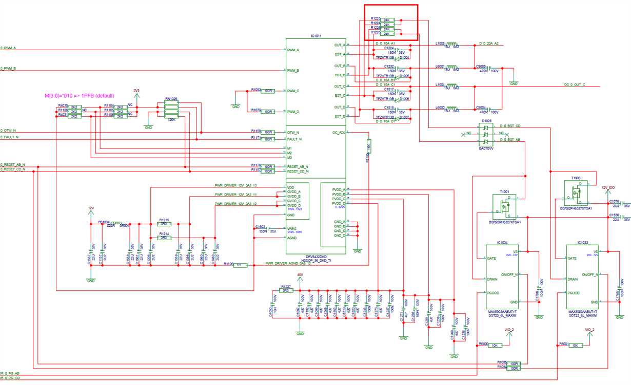
Following to the customers wish we have implemented an external bootstrap voltage option according to the TI proposal, please see the attached document. The external bootstrap voltage is isolated and related to the 48V supply.

We have noticed that when the High-Side-mosfet is ON, the output voltage of the bridge is 33V, while the bootstrap voltage is only 42V.

So we reduced 24K resistor to 2K2, we obtained 47,4V from the bridge output, and bootstrap voltage changed to 56V. So far so good.

Due to the reduced resistor value we have increased power loss when the High-Side-mosfet is OFF and the output is Low. It’s appr. 1W, because the bootstrap voltage is 13V and external 12V_ISO is 60V (seen from GND). Please find the attached schematic, the mosfet's switches below are for external bootstrap volltage while the driver is in the reset state.


Is that a wrong way to reduce the 24K resistor to 2K2? In this case we have got 1.8mA current flowing into the “BST_A” pin. What is the reason for such a high value of 24K?


Best Regards


Vitali

DRV83x2_84x2_100percent_duty_cycle.pdf

  • Hi Vitali,

    Is the 60V (12V_ISO) presented to BST_x pins when the RESET_AB_N and RESET_CD_N are high?

    Can you use the PWM_A and PWM_B to enable and disable the 12V_ISO voltage to the BST_x pins?

    If I have interpreted your schematic correctly, the BST_x pins could be subjected to higher than expected voltages when the output is low. Is that correct?
  • Dear Rick

    I will try to answer your questions on behalf of vitali, because he will be in holiday the next days...

    Yes the measurement was done with Reset signals high.

    We can not enable/disable the external bootstrap voltage with the FET Driver, because the MAX5903 has a switch on delay with approx. 180ms.

    We are surprised that the voltage drop over the 24k resistor is so high with 100% duty cycle on the PWM_x input. The 13V Z-diode should not lead much current at 12V (some nA), so our understanding is that the BST_x pin consumes 1-2mA. Is our understanding correct?

    Thanks for your support

    Best regards

    Sven

  • Hi Sven,


    Sorry for the delayed response. You are correct the 13V zener should not create that much drop.


    There appears to be an internal path that we will have to investigate. I hope to have an update by Wednesday.

  • Hi Sven,

    We have a partial update for you.

    We are still trying to determine the reason for the current flowing into the boost.

    The reason for the higher 24k resistor value was to limit the current when the output is low. A 47V drop across the resistor creates quite a bit of wasted power. Another method to limit the current is to add switches to disable the 60V to the bootstrap capacitors when the output is low.

    Is there any way you can operate the device at higher PWM frequencies? A small pulse of 50 to 100ns may be all that is required to replenish the bootstrap capacitor. This would remove the need for the additional circuitry.
  • Hello Rick,
    Many thanks for that. Sven will be in vacation for the next 4 weeks, so we have a colleague switching again. :)
    The PWM frequency is a customer requirement that we unfortunately cannot change. Pulsing bootstrap capacitor in 100% duty circle mode would have influence on the galvo position (resp. driver load).
    We appreciate your investigation about bootstrap current very much and look forward to your next update.

    Have a nice weekend!

    Vitali

  • Hi Vitali,

    Using the switch as described above (with a 2k resistor) should work, but it is recommended to disable the boost in the case of the outputs being disabled, a fault, or perhaps overtemperature warning. And you will have to deal with the power through the resistor when the outputs are low.

    In general, the device does not expect current to flow through the BST_x pins the outputs are disabled. There is no protection to disable the current through the BST_x pins to GND. This should not cause a problem, but it is a good idea to disable the path in the above conditions.
  • Hello Duncan,

    many thanks for your advice, do you know what is the actual consumer for current flowing into BST_x pin? That would be interesting for us to get more safety for that customer solution with external bootstrap voltage.

    Best Regard

    Vitali