A related question is a question created from another question. When the related question is created, it will be automatically linked to the original question.
If you have a related question, please click the "Ask a related question" button in the top right corner. The newly created question will be automatically linked to this question.
The integrated FETs of the DRV11873 already have body diodes that are in parallel with the drain and source (which serve the same purpose as flyback diodes).
Your test conditions sound good to me. Let me know if you have any other questions.
I am a beginner / amateur on electronics and motor control / design.
I have build the motor of my own design, cooling fan.
This propeller's 17 magnets have all the same polarity. (not NSNS but NNNNN or SSSSS)
9 x 3 = 27 coils are all in the same direction too.
Normally this motor is designed to work with Hall Effect sensors and a TTL circuitry. And it works very well with 16 V. 300mA.
When I tried to control it with DRV11873EVM with solar energy, it works very well too. 19,5 V solar panel: (4 x 1.5 V 100 mA) + (9 X 1.5V 250mA) and a LM2596 regulator .www.ti.com/.../lm2596.pdf
I am trying to build more of this hande made / recycled papers motors. I want to make it more efficient and lower cost.
I have already bought DRV11873 chips and necessary elements to soldier DRV11873 motor control circuits.
Do you have any suggestion about this motor and motor control circuit ?
Everything looks great, thanks for sharing. I'm glad that the DRV11873 works for you. Reducing cost by eliminating the hall sensors was a good step towards your goal.
Look into sinusoidal (180) commutation improving efficiency of driving motor with sinusoidal BEMF. This could help achieve better efficiency with the same motor.
I don't know about the motor parameters, but the DRV10974 is in a similar price range that offers sinusoidal commutation style. You'd have to look through the datasheet to see if this motor would be compatible with your motor. In addition, the DRV10974 has a higher RDSon compared to the DRV11873 which might override the efficiency gained by using a better algorithm. If I were driving motors as a hobby, I would make multiple prototypes and collect data to see which one solves the cost vs. efficiency tradeoff.
Hello Cole,
DRV10974 looks great. And 180 degree sinusoidal magnet configuration may also be a good solution for my motor configuration.
Thank you very much for your time and interest. Sure I will write if I will get a better performance.
King regards,
Oguz Coskun
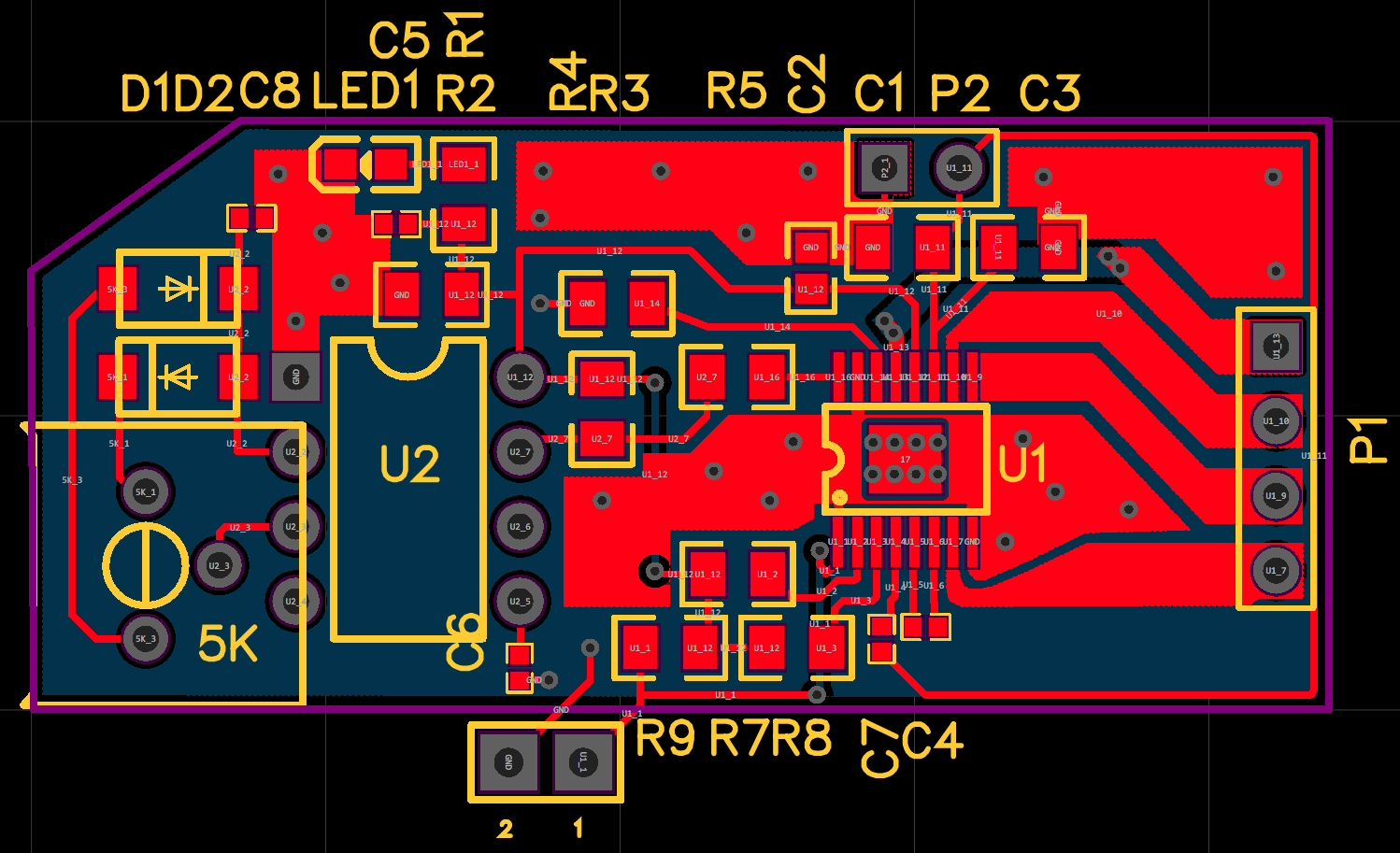
I think the layout guidelines in the datasheet does a pretty good job with what I would recommend.
A few further comments:
For example, I assume C1 and C3 are decoupling capacitors for VCC. I understand that the phase and com traces are blocking the path but I'm confident that some shifting could allow you to move the decoupling capacitors closer. If the device demands more charge from VCC, right now, the charge has to go through 2 vias (which is stray, series inductance) and a longer trace (which is more resistance) until the charge can be delivered to the device. And the GND potential all has to go from the GND pin, through some more vias, then to the other side of the capacitor. You can think of this as an LC circuit where high frequencies (e.g. fast demands for current) will resonate and cause spikes that can disrupt the rest of the circuit. While it may work in this design, good layout technique prevents something like this from happening. You should consider this for the other important capacitors as well.
Also, I do not see a ground pour (or the bottom layer). Right now it looks like the power pad is floating (because there are not vias and it is not connected to pin 8, GND). The power pad dissipates heat and allows charge to spread out so it does not create a potential difference between two points on a GND plane. Consider putting a large pour on the top and bottom with many vias stitching the grounds together between the two layers.
My only concern is that the powerpad (looks like net 17 on your routing view image) still doesn't look connected to the large top layer GND pour. The powerpad or Die Attach Paddle (DAP) should be connected directly to the GND pour. This way the GND pour will be covering the PowerPad and look just like the GND pin of C1 and C3.
If you have any more questions or would like to remind me to answer some of your unaswered questions, let me know by replying to one of the posts in the thread. If the question is related to the project but not related to the layout, I encourage you to make a new thread and post a new question.