Other Parts Discussed in Thread: DRV8353
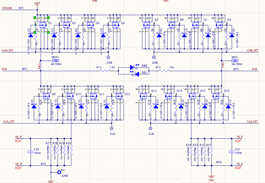
Hi. I am using the DRV8353RH in a high-current motor-control application which requires multiple, paralleled FETs to keep the Rds power dissipation down. Adding the FETs has increased the total gate charge and the math is telling me I need to increase my gate drive beyond what the IC is normally capable of. On the low-side, I think I'm in good shape. Insert a FET driver on the low-side gate lines, power the driver off of VGLS, ensuring the current doesn't exceed the 25mA available, and (conceptually) I'm good to go. The high-side (HS) has me a bit confused, however. Normally, I would expect the HS drive voltage to be referenced to the source of the upper-half N-FET. In this way, we'd always have ~12V to put across Vgs for turn-on. On the DRV8353 however, the charge pump/HS voltage is referenced to the HS FET drains. I suppose this allows the use of only a single charge pump across 3 half-bridges, but I'm at a bit of a loss as how to wedge additional gate drive in here. Any thoughts?


