This thread has been locked.

If you have a related question, please click the "Ask a related question" button in the top right corner. The newly created question will be automatically linked to this question.

DRV8847: Questions for DRV8847S I2C Waveform

Part Number: DRV8847

Hi Experts,

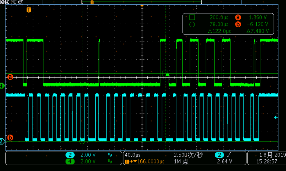
Recently our customer is debugging on our DRV8847S on their board, and captured some strange I2C SDA line waveform as below, where you will see a bar when voltage goes from high to low. Also we checked some application notes for this device, and saw one waveform looks like similar to customer's behavior, but not sure(http://www.ti.com/lit/an/slvae40/slvae40.pdf). Do you have any thoughts why there is a bar in here?

1. Strange I2C SDA line waveform captured on customer's board:

2. Looks like there is a similar behavior captured in this application note, but not sure:

Thanks a lot!

  • Hi Jacky,

    Would you kindly send me a waveform showing the SCL and SDA for the moment when the bars are showing up? 

  • Hi,

    This is the schematic of MCU and DRV8847S connection.

    This is the SDA and SCL waveform at DRV8847S side. Green-SDA, blue-SCL.

    This is the SDA and SCL waveform at MCU side. Green-SDA, blue-SCL.

  • Hi Jacky,

    Thank you for providing the waveforms and schematic. I will have to do further investigation to figure out what is causing those bars in the SDA signal. 

    You should expect a response by Tuesday/Wednesday of next week. 

  • Hi Pablo,

    Any findings for this issue? Customer is waiting for our feedback.

    Thanks.

  • Hi Jacky,

    I am sorry for the delayed response. There might be a BUS contingency occurring. As you can see in the block diagram below, the SDA has an open drain FET which pulls the SDA signal to ground when ON. On the other side of the SDA, the signal is connected to the MCU which is able to pull or push the signal. If the MCU is trying to drive the SDA signal while the FET is pulling the signal low, the SDA can be in a state between high and low for some time similar to what the customer is seeing.

    To verify if this is correct, can the customer take the voltage waveforms at the locations marked in the schematic below? Specifically, I would like to see the voltage values at those locations when the "bars" are appearing on the SDA signal. 

    Thank you for your patience. 

  • Hello,

    The schematic was not attached correctly. Here it is.

  • Hi Pablo,

    Note that the customer has changed R74~R76 and R80~R82 values from 1kOhm to 100Ohm when below waveforms were measured.

    Picture1 is the SDA waveform at the left side of R75. The SDA bar voltage is 1.36V.

    Picture2 is the SDA waveform at the right side of R75. The SDA bar voltage is 3.8V.

  • Hi Pablo,

    Below waveforms are tested when R74~R76 and R80~R82 are 1kOhm. The bar voltage is changed according to the resistors values.

    Picture1 is the SDA waveform at the left side of R75. The SDA bar voltage is about 0.2V.

    Picture2 is the SDA waveform at the right side of R75. The SDA bar voltage is about 4.8V.


  • Hello Rui,

    I am convinced now that there is a BUS contention (sorry for misspelling on my previous reply) occurring. With resistor of 100Ω, the MCU side is trying to drive the SDA pin while the open-drain FET in trying to pull the SDA low. 

    I would start by telling the customer to configure the MCU pin as open-drain rather than push-pull configuration. This will eliminate the BUS contention. If the customer can, they can reduce the 10kΩ pull up resistor down to 2kΩ and use that to pull the SDA high. 

    I hope this explanation makes sense. 

  • Hello,

    We have moved the discussion of this thread to another external means of communication. Therefore, I would like to close this thread.