Other Parts Discussed in Thread: DRV8353R, ISO7761, ISOW7841, SN6501
Is the gate driver DRV8353R isolated or not? If not, What are the impacts of using it without isolation and how can we provide external protection or isolation.
This thread has been locked.
If you have a related question, please click the "Ask a related question" button in the top right corner. The newly created question will be automatically linked to this question.
Is the gate driver DRV8353R isolated or not? If not, What are the impacts of using it without isolation and how can we provide external protection or isolation.
Thank you for replying,
I want to understand, is the MCU ground isolated from the system ground; and if not, what is the effect of this?
Shaza,
The DRV GND is connected directly to the FET bridge GND. You can isolate the MCU from the rest of the system if you choose.
The reason the DRV is connected directly to the FET bridge is because this is how the DRV monitors the FETs and also how the DRV drives current into the FET gates and similar.
Regards,
-Adam
Adam,
We have digital isolators capable of isolating the 12 digital signals between the MCU and DRV. Unfortunately our digital isolators would not be able to isolate the current sense amp outputs (SOA, SOB, and SOC). For the isolating the digital signals, I recommend using two ISO7761 devices. Are you familiar with digital isolation in regards to PCB design and power supply?
Respectfully,
Lucas
Hi Shaza,
Hopefully all is well. Would you still like assistance isolating digital signals between the MCU and DRV as mentioned above? Current sense measurements can be isolated with Isolated amplifiers TI offers as described in this TI Design. Please let us know soon to prevent this thread from being closed due to inactivity.
Thank you for your time,
Manuel Chavez
Could you please help with the digital isolation in regards to PCB design and power supply? I would appreciate very much.
Hi Shaza,
Of course!

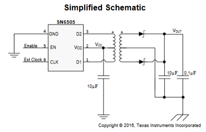
Isolated power supplies can be derived based on your application's isolated load requirements: what is the estimated current load? For an isolator that can power itself and supply ~120mA for additional ICs, the ISOW78xx family of devices (including ISOW7841 shown above) might simplify the design, and for higher power requirements (1.75W - >5W), isolated power supplies can be designed using isolation transformer drivers like TI's SN6501 and SN6505. These devices are typically used as shown below:
Please let me know if this information is helpful for your design.
Thank you for your time,
Manuel Chavez