


Other Parts Discussed in Thread: , CSD18531Q5A, CSD88537ND,
Hello,
I am trying to figure out how to design a circuit with the DRV8711 that will respect the absolute maximum ratings of the DRV8711.
If I focus on the ratings for the "Phase node pin voltage (AOUT1, AOUT2, BOUT1, BOUT2)" I see the rating for the pins are between –0.6 and VM + 0.6 V. My concern is when the system is in a high impedance state where all of the bridges are disabled, for instance during a dead time cycle, the body diodes of the MOSFETs will conduct if there is current flowing through an inductance. When the current is being sourced from a low side fet through the body diode as well as the low side sense resistor. It seems very difficult to stay within the -0.6 rating on these pins given the forward voltage of the body diode on top of the sense resistor voltage drop.
To work an example lets use the DRV8711EVM:
Assume a modest operating current of 1A.
From the CSD18531Q5A datasheet we see the forward diode voltage is:
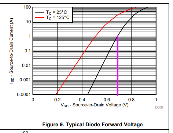
0.68V
Next we calculate the voltage drop over the sense resistor:
0.033 Ohms * 1.0 A = 0.033V
Now summing the voltage over both the sense resistor and the body diode we have:
0.68 V + 0.033 V = 0.713 V.
Ooops, we have violated the maximum ratings of the DRV8711 with the body diode forward voltage alone.
Are the absolute ratings correct for those pins? If so, how does TI recommend we stay within the absolute ratings when the vast majority of body diodes have a forward voltage of 0.6 V at 1A alone?
Thanks,
Allen


