This thread has been locked.

If you have a related question, please click the "Ask a related question" button in the top right corner. The newly created question will be automatically linked to this question.

DRV8711: Gate driver damage and reset/disabled/unconnected drive damage

Part Number: DRV8711

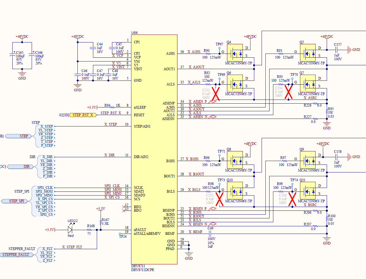
We are having two issues with our implementation of the DRV8711.

First we are seeing somewhat frequent damage to the gate drivers of the DRV8711, it seems more frequently the low side drivers are experiencing damage. The damage is measured by measuring the gate driver impedance to ground. Typical/unused DRV8711 low side gate drivers have an impedance of ~150kOhms to ground, high side around 500kOhms. What could be causing this damage to the DRV8711? We don't measure any violation of the absolute maximums of the part so far on the gate drivers. Is there anything we should review or measure that might lead us to the source of the damage? The FETs appear to be unaffected/undamaged in this scenario.  

We also are experiencing driver damage and FET damage but we are extremely confused because:"

  1. we don't have a load attached to the power stage
  2. The DRV8711 doesn't appear to ever get enabled via SPI (CS is always low)
  3. The DRV8711 is held in RESET via the RESET pin relatively soon after power up (SLEEPn is always pulled high)

What could be causing such failures and damage to both the FETs and DRV?

Could transients on the AOUTx/BOUTx or ISENSEx pins cause damage to the gate drivers, particularly the low side drivers?

Here is the schematic:

  • One other note. We have switched the MOSFETs to be ST BSC440N10NS3 G and the gate resistors to 200Ohms. I understand that there may be some concern around dv/dt effects possibly turning on the lowside FETs when the high side FETs turn on but we haven't seen this and have measured the voltages to be below the threshold voltage.

  • Hi Allen,

    The only suspicious thing I noticed on your diagram is a bit low R168 resistance, I don't know max current

    for FAULTn output but 14-20mA seems a bit high.

    Best Regards,

    Grzegorz

  • Hi Allen,

    Can you provide a little more information?

    What are the register settings used? When using 100 Ohm low side gate resistors, "TI also recommends setting the dead time to 850 ns when adding a series resistor."

    Is it possible there are voltage spikes on VM that approach/exceed 60V?

    Have you tried removing the high side gate resistor? TI has not seen the need for high side series gate resistors.

    As Grzegorz stated, R168 is lower than expected. Please limit the current to 5mA through the LED. Limiting the current will ensure the FAULTn pin is interpreted correctly by the mcu.

  • We are using the following settings on the drivers that are experiencing gate drive damage. Note the current is in units of Amps and the sense resistor in units of Ohms.

    // Drive 1 - 2 
    // Note all drives have dead time set to 850ns DTIME=0x3, ISGAIN=0x1, EXSTALL=0x0. { 1.2 // Active Current , 0.35 // Idle Current , 0.05 // Sense Resistor , true // Direction Bit , DRV8711_USTEP::ONE_TWENTY_EIGHT_STEP , 0x10 // Default TOFF , 0x32 // Default TBLANK , false // Disable adaptive blanking period , 0x30 // Default TDECAY , DRV8711_DECAY_MODE::FAST_ALWAYS , 0x0040 // Default stall register , DRV8711_OCPTH::OCP_500mV , DRV8711_OCPDEG::OCPDEG_4us , DRV8711_TDRIVE::TDRIVE_250ns , DRV8711_TDRIVE::TDRIVE_250ns , DRV8711_IDRIVEN::IDRIVEN_100mA , DRV8711_IDRIVEP::IDRIVEP_50mA}; // Drive 3
    { 0.5 // Active Current , 0.35 // Idle Current , 0.05 // Sense Resistor , true // Direction Bit , DRV8711_USTEP::SIXTEEN_STEP , 0x40 // Default TOFF , 0x32 // Default TBLANK , false // Disable adaptive blanking period , 0x30 // Default TDECAY , DRV8711_DECAY_MODE::SLOW_MIXED , 0x0040 // Default stall register , DRV8711_OCPTH::OCP_500mV , DRV8711_OCPDEG::OCPDEG_4us , DRV8711_TDRIVE::TDRIVE_250ns , DRV8711_TDRIVE::TDRIVE_250ns , DRV8711_IDRIVEN::IDRIVEN_100mA , DRV8711_IDRIVEP::IDRIVEP_50mA}; // Drive 4 - unprogrammed, held in reset.
    // Note all drives have dead time set to 850ns DTIME=0x3, ISGAIN=0x1, EXSTALL=0x0.

    Note we aren't programming one of the drivers that isn't connected to a load and left in reset.

    We never see the FLT led on during normal operation. We will make the change to limit the current.

    We have a 600w-1000w 48v meanwell supply that we have never observed going out of regulation or having spikes.

    We have added the high side gate resistor to limit the dv/dt for EMC and to reduce the chance of parasitic turnon of the low-side FETs.

  • Yesterday we had another drive fail. This was a new failure mode where a drive experienced shoot-through destroying a half-bridge and the gate drivers. This was one of the programmed drives. There is some indication that this may be due to power up or power down though it isn't certain at this time. 

    What is the impedance of the gate drivers when:

    1. Powering up
    2. Powering down
    3. DRV8711 Disabled in reg 0
    4. DRV8711 RESET asserted

    Additionally the drives are initialized by writing to reg addr 1-6 in order and then to 0 to enable the drive.

  • Hi Allen,

    Thanks for the information. I have a couple of additional questions for now and then will start investigating.

    On which drives are you seeing FET failures? If only one which one? This could help isolate to programming or layout.

  • Rick,

    Some additional information that may be pertinent:

    1. We have 4 drives on one board with more or less identical layouts.
    2. We have had gate driver failures of all 4 drives.
    3. So far we have only had one shoot through failure.

    I will review the boards to see if there is any commonality to the failed drivers.

    I can PM the design files if that would be helpful (Altium which I believe you use).

  • Hi Allen,

    Yes, it is always helpful to check the layout. We will make arrangements to receive the files. Altium is preferred.

    Are you saying that the drive that is not used had FETs that failed? That may provide a clue. Also, please provide the designators of FETs that have failed to date.

    I found some information on the low side drive impedance:

    When xLS outputs are
    Powered off -- passive connection to ground through a nominal 150kOhms to ground
    Powered, sleep mode -- actively pulled to ground through a nominal 12mA driver
    Powered, awake, reset -- actively pulled to ground through a nominal 63mA driver

  • Rick Duncan said:

    Are you saying that the drive that is not used had FETs that failed? That may provide a clue. Also, please provide the designators of FETs that have failed to date.

    Yes, there is a drive that has never been connected to a load that has had DRV gate drive damage. In theory this drive is never enabled via SPI and for most time has RESET asserted.

    Is there any information on the low side drive impedance when the drive is disabled i.e. bit zero of reg at addr zero is zero. Said another way ENLB in the CTRL register is always zero.

    I will have the designators of the FETs failed to date shortly. I will also provide designators of the FETs that have DRV gate drive damage.

  • Here are the impedances measured to ground on the DRV side of the gate driver. 

    Board A Board B Board C Board D
    Q6 109k Q5 227k Q5 291k Q4 420k
    Q10 145k Q7 88k Q7 120k Q6 137k
    Q21 430k Q8 230k Q8 197k Q8 450k
    Q23 99k Q22 280k Q10 127k
    Q24 136k Q24 117k Q15 182 (DRV short, not gate)
    Q27 138k Q25 380k Q32 134k
    Q29 255 (DRV short, not gate) Q36 273 (DRV short, not gate)

    Interestingly Q4-Q11 are all on the drive without a load that we do not believe we are programming and is being held in reset after boot.

    I will send the full schematics and PCB layout shortly.

    One thing to note if anyone else sees this in the future the high side measurements are dependent on the meter you use. I used a Fluke 179 to get these measurements.

  • Board E
    Q6 144k
    Q13 224 (Gate short)
    Q15

    205 (Gate Short)

    I realized I was missing the board that had the FETs that experienced shoot through. Q13 and Q15 are shorted to GND and completely destroyed. 

    I would also like to reiterate that the schematics call out the wrong FETs and gate resistors the FETs are all ST BSC440N10NS3 G and the gate resistors to 200Ohms on all boards and all drives.

  • Hi Allen,

    I use Mean Well 480W 48V power supply myself and I know it can give quite a big spark (ie, current) when connected

    powered to my DRV8711 board (my board has around 10000uF bulk capacitance between VM and ground) so I keep

    board connected to power supply when turning power supply ON.

    Do you connect your board to 48V power supply when its ON, by contactor for example or keep them

    connected all the time?

    DRV8711 may not like high dV/dt on VM. It is just my another guess.

    Below there are settings for my DRV8711 board that I've used for the last 1,5year, I use FETs from DRV8711 EVM board, sense resistors 10mOhm,

    currents usually 4-6A but tried for a couple of seconds up to 20A several times (I don't remember if used GAINx10 or GAINx5 back then)

    DTIME850

    GAINx10

    DECAY_AUTO

    IDRP_150;
     
    IDRN_300;
     
    TDRP_500;
      
    TDRN_500;
      
    OCPDEG_2;

    OCPTH_500;
      

    Best Regards,

    Grzegorz

  • Grzegorz,

    We are not hot-plugging the system. The power up and power down happen with the supply connected and appear monotonic over a fairly long time frame.

    Since our motors and MOSFETs are different I don't think the drive currents and decay mode are directly comparable.

    Are you using gate resistors at all? The EVM board FETs are TI parts which have very good dv/dt characteristics but have too high of gate charge for our switching frequency (upto 80kHz) since our motors have low inductance (~2mH).

    Allen

  • Allen,

    I just missed two parameters

    T_OFF = 0x40 - I've set the lowest possible PWM frequency to limit power losses and just not to hear switching noise to much.

    T_Blank = 0x80

    I use just low side gate resistors 56 Ohm each, I don't use high side ones.

    At the moment I use Nanotec ST6018D4508-A that has parallel inductance  of 1.4 mH but I drive that motor at high currents,

    maybe it is the reason I can use low PWM frequencies.

    I set initially DRV8711 registers after 12-20 ms after power up keeping Reset and Sleep pins low.

    Grzegorz

  • Allen,

    I just checked my program, I don't use DRV8711 Reset pin, I keep it low all the time, I use only Sleep

    pin to turn off DRV8711 when I don't need it.

    Grzegorz

  • Allen,

    Just a few more thoughts.

    There are two things that may suggest possible VM problem.

    - all 4 drives share the same VM bus I guess, if there was an overvoltage it would cause failure of any drive, even the one unused

    - BSC440N10NS3  is 100V rated Mosfet and would be less likely to fail in case of VM overvoltage unless DRV8711 turned both LS i HS Mosfets ON at the same time

    Power supply 600W-1000W is very powerfull for 3 motors around 1A each, do you use that power supply to supply more drives or other devices?

    Motor drives including stepper motor drives can give power back to VM bus increasing its voltage.

    In case of stepper motors I noticed that they give power back to VM bus during motor resonances and during braking (especially braking from high speeds or

    braking loads during moving them down either in controlled way or not). I decided to use 10000uF capacitance to store energy from Nema 24 i 34 motors

    in case of any resonance and light braking, for uncontrolled braking from high speeds I had to add breaking chopper.

    Unless you are 100% sure that VM does not experience any overvoltages I would try one or more of steps below:

    - add more capacitance to VM

    - replace power supply with another one, 200W should be enough for these 3 motors, use it only for that 4 motor drive

    - monitor VM voltage all time for max voltage

    - add some protection circuit, I posted some 2-3 months ago diagram of breaking chopper but with currents around 1A

    it would be overkill unless you drive some heavy weights up and down.

    Do you use any motor output EMI LC filters?

    There is some small chance that they can cause some electrical resonances.

    Grzegorz


  • Grzegorz,

    1. Initially I have not seen any overvoltage conditions exceeding VM by more than a diode drop. I will review more this coming week.
    2. Our system has many other components in it. We limit the 600w supply to only supply 6A via a fuse to the board.
    3. The supply is always attached, no hot-plugging.
    4. I tested backdriving and was unable to exceed 24v in our application so I don't think a shunt is necessary.
    5. We don't use EMI LC filters on the output

    Allen

  • Rick,

    1. What power sequencing requirements do the DRV8711 have?
      1. If there is activity on the logic inputs before VM is fully stabilized is this a violation?
      2. Are there requirements on the logic input pin states during power up of VM?

    2. Is it possible to program the DRV8711 with bogus data if the SPI doesn't complete the transactions per the datasheet requirement?
      1. What happens if SCS becomes high but doesn't persist for SCLK rising edges bits?
      2. What happens if SCS becomes high but there aren't any SCLK transitions during the SCS high period?

    Thanks,

    Allen

  • Allen,

    I just used scope to take a look at my startup sequence and it is much more complex than I thought.

    Rump up of VM from 0V to 48V takes around 55ms.

    At about 30V start step down converters supplying MCU.

    At about 36V Reset, Sleep and Clk goes high (I don't know if it is caused by MCU or DRV8711, according to program Reset an Sleep should stay low but the program probably

    hasn't started yet), SCS stays low at that time.

    VM goes to 48V.

    About 45ms after VM reached 48V Reset, Sleep and Clk goes low, SCS is still low. Reset from that point is always low.

    About 60ms after VM reached 48V initial setting of Registars starts, ENBL bit in CTRL Register is 1.

    Startup sequence is descibed in some way in DRV8711 EVM manual.

    Grzegorz

  • Hi Allen,

    1. What power sequencing requirements do the DRV8711 have?
      1. If there is activity on the logic inputs before VM is fully stabilized is this a violation?
      2. Are there requirements on the logic input pin states during power up of VM?

    1) There are no power sequencing requirements.

    1a) It is not a violation if there is activity on the logic inputs before VM is fully stabilized. The SPI transactions may be ignored.

    1b) There are no requirements on the logic inputs during power up.

    Was originally numbered 2

    1. Is it possible to program the DRV8711 with bogus data if the SPI doesn't complete the transactions per the datasheet requirement?
      1. What happens if SCS becomes high but doesn't persist for SCLK rising edges bits?
      2. What happens if SCS becomes high but there aren't any SCLK transitions during the SCS high period?

    1) We are not aware of the possibility. Are you concerned about a specific scenario?

  • For #2

    Our concern is the process that provides logic input takes significantly longer than the time it takes for VM to stabilize so we get spurious signals on the SPI bus and wondered what would happen if an incorrect number of SCLK cycles occurred while SCS was high. Could it latch garbage data into the chip resulting in a mis-configuration.

  • Hi Allen,

    We have checked the list of reported problems, and have not seen this issue.

    The device should be operational ~1ms after VM is >UVLO (~8V), nSLEEP is high and RESET is low.

    When are you starting SPI transactions?

    I was also able to contact the designer. He is not aware of any issues that would cause device damage.

  • I am concerned primarily about spurious SPI transactions due to noise in the system.

    When the system is powering up the SCS and RESET lines aren't well defined which is why I am curious what happens when SCS isn't high for a full 16bit transfer. 

    Were there any suggestions from the designer of what _could_ cause damage, not what normal operation would allow for?

  • Hi Allen,

    The designer did not have a.ny suggestions of what could cause the damage.

    I will send a private message to you in a few minutes.

  • Hi Allen,

    This post will be marked as "TI Thinks Resolved" as the last conversations were private.

    You can still use the post until it is locked for any generic questions/updates.

  • Hello, Can you describe what was causing the issue, and the solution offered for the same? I have a similar implementation in progress using DRV8711 and the information would be helpful.

  • Hey Anshul,

    We have not yet determined the true root cause of the issue(s). Effectively we have two problems:

    1. Drives we believe are never enabled getting damaged. They also don't have a load attached.

    2. Drives we enable with loads getting damaged.

    We have a possible explanation for 2. When the DRV8711 powers on or wakes up from reset the default values of the registers are unsuitable for most applications. For our application the TORQUE register is way out of specification for anything we would drive and ends up commanding >10A of current through the attached motor. Our mistake was programming the DRV8711 registers in sequence from 0->6 thereby enabling the drive before the remaining parameters of the DRV8711 were set. This caused the drive to operate for a brief period (~10ms?) where we believe the damage to the enabled drives was occurring.

    For 1. we wondered if it was possible the drive was getting spuriously enabled but haven't gotten a clear indication if that is possible.

    To help mitigate general issues we have done the follwoing

    1. Added gate resistors to all FETs (TI has recommended against adding gate resistors to the high side FETs but we are having EMC issues and simulations have shown other desirable characteristics)

    2. Added a resistor and schottkey diode pointing from the gate to the gate drive pin of the DRV on the low side to protect against parasitic turn on

    3. Added a clamping schottkey diode from ground to the gate to prevent negative voltages from developing on the gate to respect the absolute ratings of the part

    4. Added gate to source resistors on all FETs to prevent the buildup of static charge that could enable the FETs

    5. Added schottky diodes to the phase nodes (AOUTx, BOUTx) to prevent negative voltages from developing via the forward voltage of the body diode and the source sense resistor to respect the absolute ratings of the part.

    6. Added snubbers to the phase nodes to limit the dv/dt of the phase node voltage to reduce the chance of parasitic turn on and help with EMC

    7. Added circuitry to ensure the RESET line was active until explicit positive action was taken by the controlling processor to enable the drives to prevent any possible spurious enabling of the drive.

    The FETs we used have relatively total low gate charge (10nc), our application is at 48v, and we are running ~2A through the motors so these precautions may be grossly excessive for your application.

  • We will be receiving boards with the above changes later this month and I will report back the results.