This thread has been locked.

If you have a related question, please click the "Ask a related question" button in the top right corner. The newly created question will be automatically linked to this question.

DRV2625: DRV2625 VDD versus LRA waveform Vpp

Part Number: DRV2625
Other Parts Discussed in Thread: DRV2605, DRV2624

Hi

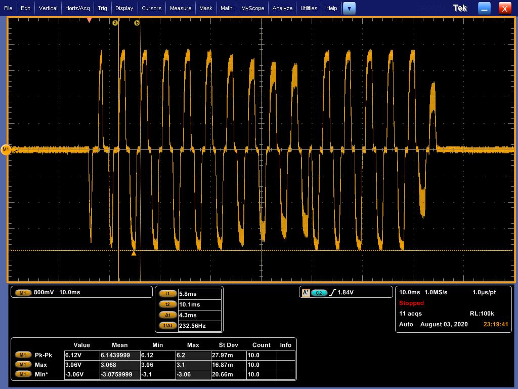
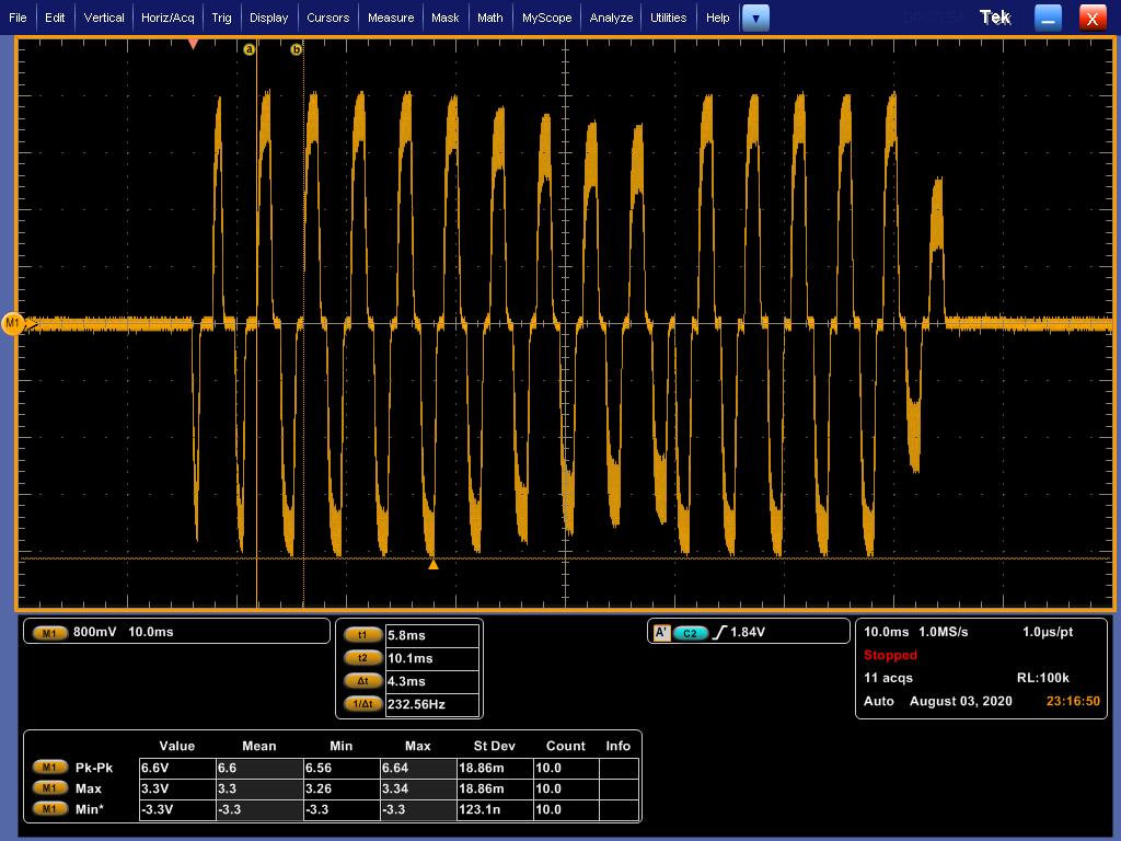
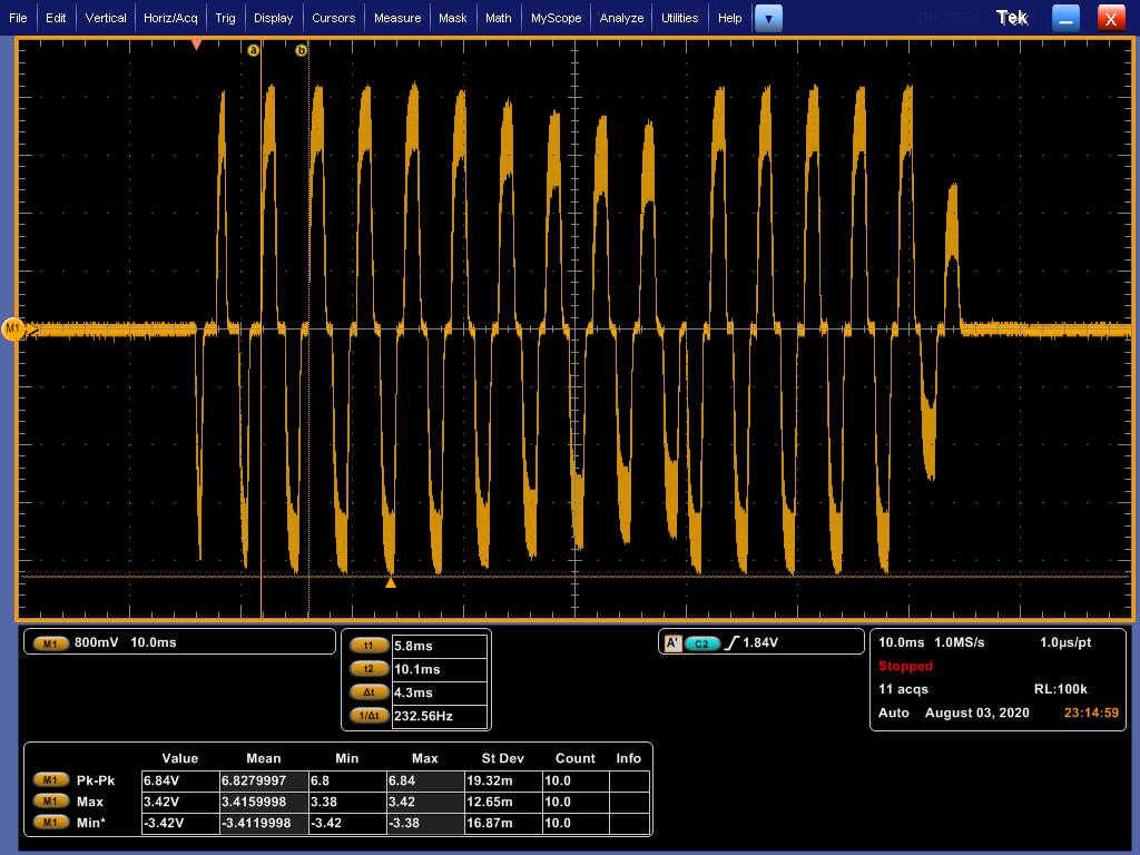
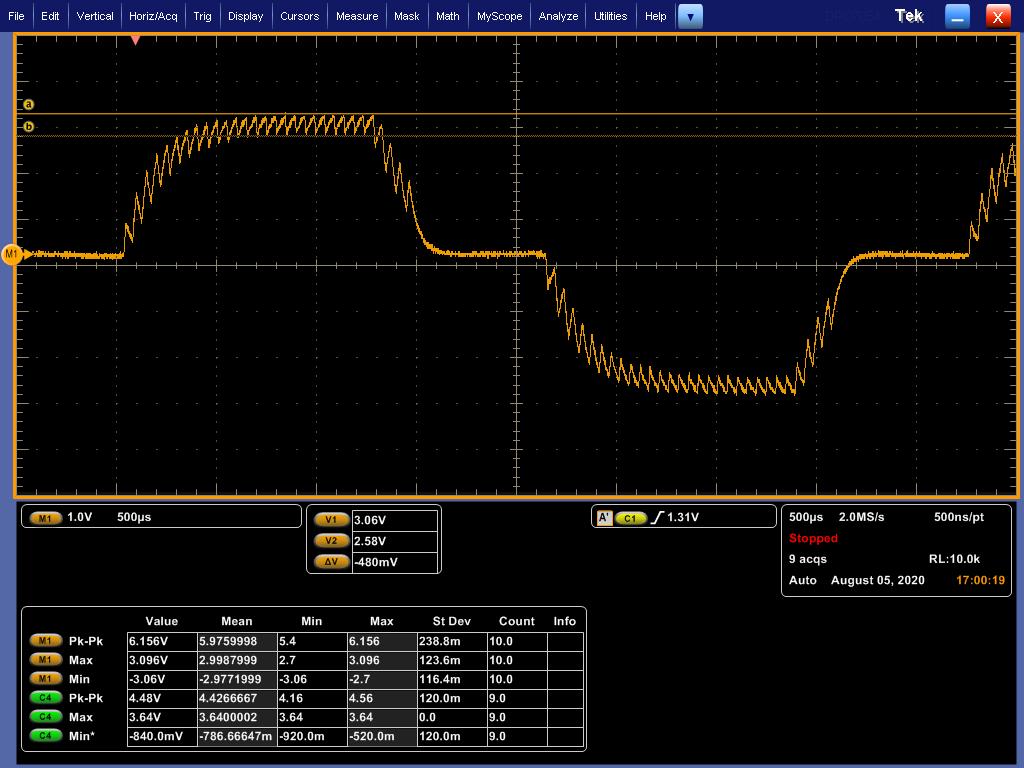
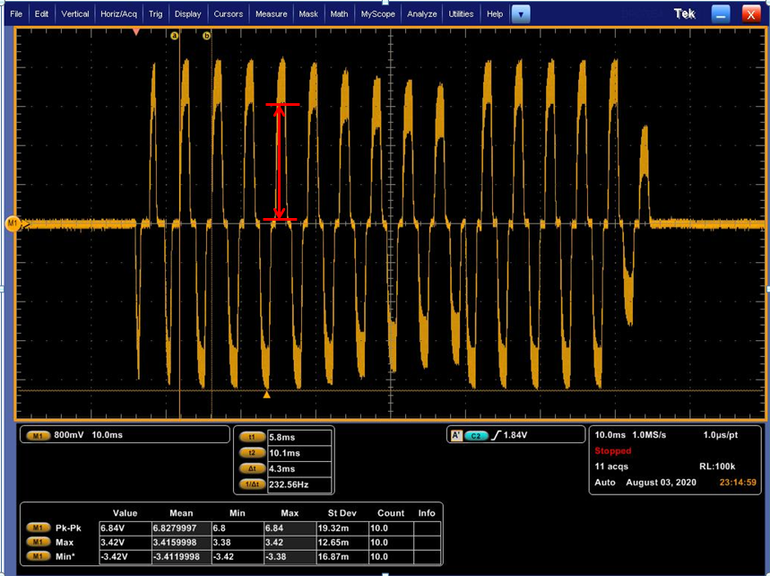
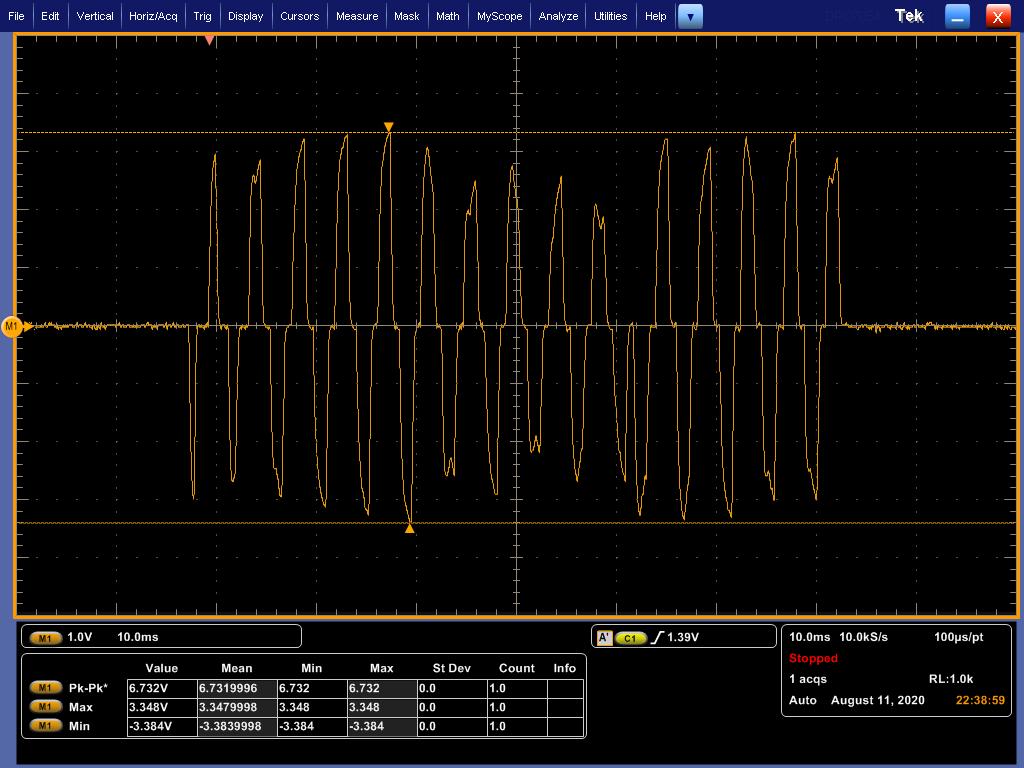
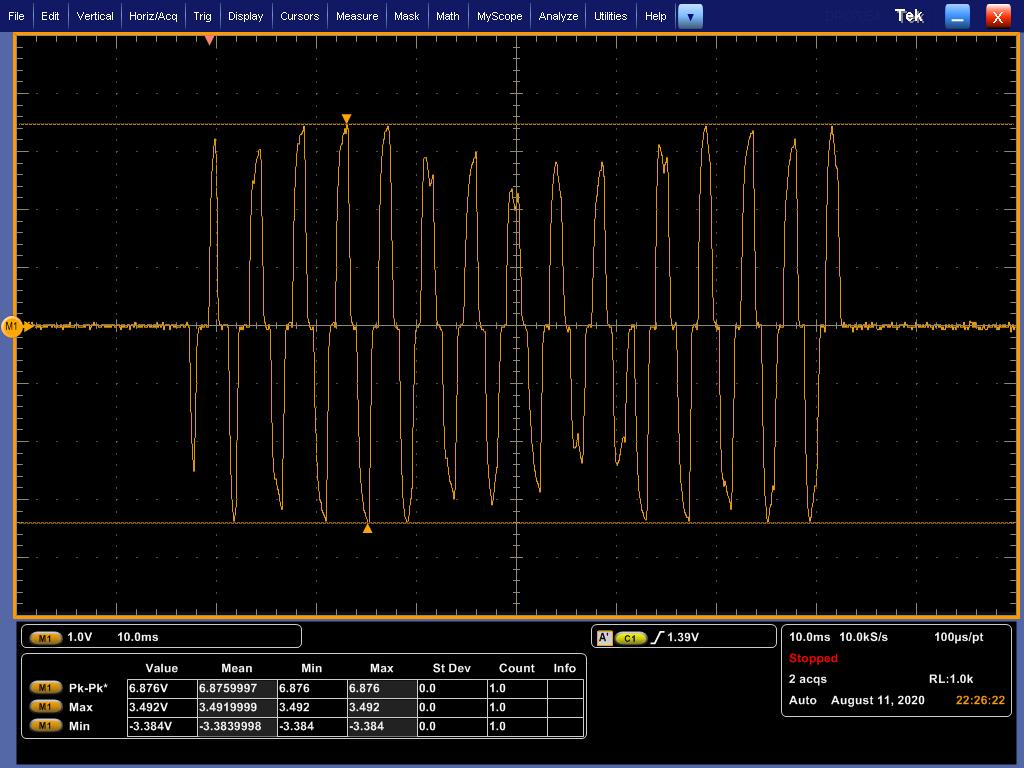
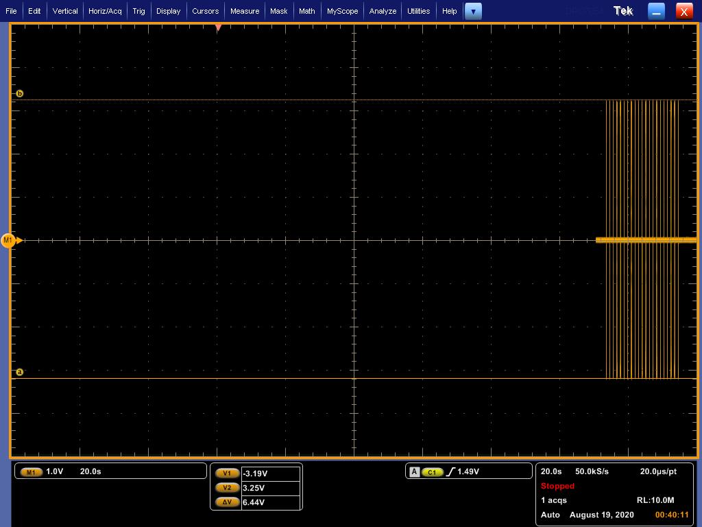
We set overdrive voltage = 3Vpeak as attached excel

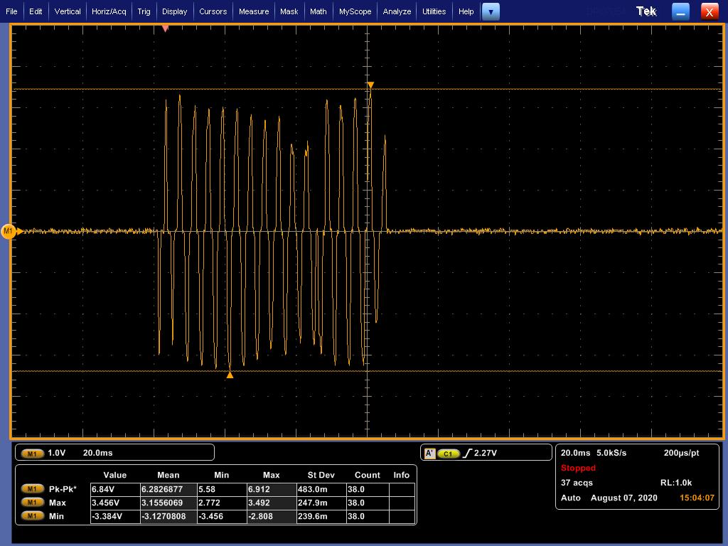
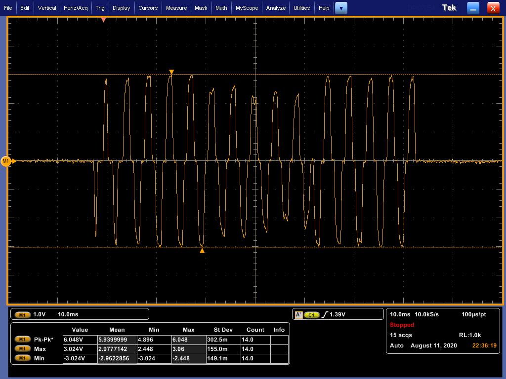
But we find when we change DRV2625 VDD voltage, the waveform Vp/Vpp also change as below table

Is it normal? Since as I know the Vp should limit at Vpeak setting

Thank you~~

Haptic_VDD(V) Waveform Vp(V) Waveform Vpp(V)
4.4 3.42 6.84
4.2 3.34 6.68
4 3.3 6.6
3.8 3.22 6.48
3.6 3.14 6.32
3.5 3.1 6.2
3.4 3.06 6.12

8132.DRV2624 and DRV2625 Configuration Tool and Design Equations-AWA_modified.xlsx

  • Hi, Poki,

    Are you modifying the VDD level after the DRV2625 has been configured? I mean, could you verify if you get different results under the tests below?

    - Set the VDD level, then configure the device. Measure the Vp and Vpp level. Power down the device and change the VDD level to see the difference.

    - Set the VDD level, then configure the device. Measure the Vp and Vpp level. Modify the VDD level without power down the device to see the difference.

    Please let me know if you have questions or comments on this.

    Best regards,
    Luis Fernando Rodríguez S.

  • Hey Poki,

    It should not be going past 3V if that what the clamp voltage is set at, I will run some tests on my own to see if I come up with a similar pattern. From the other threads we have been discussing I know you have multiple chips, are they all showing these results? Is the rated voltage acting as it should?

    Also are these values with an LRA attached?

    Best,

    Carson

  • Hi Luis:

    I do both test and get the same result as above table

    Have you check attached .xlsx file? Any problem about it?

    Thank you~~

    Poki

  • Hi Carson:

    Yes I test another chip and get the same result, Vp/Vpp level change with VDD level with above two setup, those test attached LRA

    (- Set the VDD level, then configure the device. Measure the Vp and Vpp level. Power down the device and change the VDD level to see the difference.

    - Set the VDD level, then configure the device. Measure the Vp and Vpp level. Modify the VDD level without power down the device to see the difference.)

    And the rated voltage(Vrms) should increase with VDD increase since the waveform shape not change, only change Vp/Vpp, I attached some as below

    Waveform is strong click 100%

    VDD=3.4V

    VDD=4V

    VDD=4.4V

    Poki

  • Hey Poki

    I think your problem might be due to the fact that you are too zoomed into you oscilloscope and are picking up a lot of the PWM noise which is the all fuzziness at the peaks of the wave forms. If you zoomed out and then took measurement of the peaks it may give more consistent result that at your OC_CLAMP voltage.

    So measured with a large time division and show and examine those results

    Also are you making sure to either auto-calibrate or reload in the calibration value settings from the host processor every time you turn on and off when you change VDD.

    Best,

    Carson

  • Hi Carson:

    Yes when we change VDD, we turn off system, setting VDD, and turn on system.

    We check PWM signal (before low pass filter) with VDD=3.6V and 4.4V, we found the Vp will increase with VDD and the Vp is almost equal to Vp as below chart

    Is it normal or not? If not, seems our OC_CLAMP=3V didn't work, have you check attached .xlsx file and if any wrong?

    VDD=3.6V, measured Vp=3.54V (by cursor)

    VDD=4.4V, measured Vp=4.38V (by cursor)

    Also we check waveform top detail (after low pass filter) and find there is PWM signal inside

    We use your DRV2605 EVB low pass filter (100Kohm and 470PF)

    Is it normal?, If yes, the ripple high and low gap is ~480mV, which one should we use to calculate Vrms?


  • Hi Carson:

    Could you help do same test that setting RATED_VOLTAGE=1.8V, OC_CLAMP=3V, and change VDD=3.6V and 4.4V to see waveform Vp level?

    Thank you~~

    Poki 

  • Hi Carson:

    Sorry add one question

    You said there's PWM noise on top of waveform

    So you mean we take below chart red arrow area as Vp?

  • What I am saying is when you have it zoomed in like you do you see ripple from PWM which will make the waveform look like it is going above my clamp voltage of 3V.

    Where as if you zoom out on this same waveform that switching frequency is not picked up and see that the waveform is not going past 3V like this:

  • So when trying to calculate Vrms and Vpeak try to freeze it at a large time scale and zoom in so the PWM is not being picked up and it looks like this:

    Try doing that and see if you get it to obey your clamp voltage setting even when you vary the VDD.

  • Hi Carson:

    We decrease sampling rate to 5K/S and find the PWM noise disappear

    Our setting is rated voltage = 1.8V, clamp voltage = 3V

    We change VDD 3.6V and 4.4V and the Vpp still change as below chart(VDD=3.6V, Vpp=6.192V; VDD=4.4V, Vpp=6.84V)

    What is your VDD setting in the previous test you provide?

    And please help change VDD=3.6V and 4.4V on you side to see Vpp status

    And if your test, Vpp won't change with VDD, which setting or anything we need check? Did you check our setting file(excel)?

    Thank you~~

    VDD=3.6V

    VDD=4.4V

  • Hi Carson:

    We decrease sampling rate to 5K/S and PWM noise disappear

    Our setting is rated voltage = 1.8V , clamping voltage = 3V

    We change VDD 3.6V and 4.4V but Vpp still change (VDD 3.6V, Vpp=6.192V; VDD 4.4V, Vpp=6.84V)

    What is your VDD voltage setting at previous test you provide?

    And please help do test that change VDD 3.6V and 4.4V on your side to see Vpp status

    If your test, Vpp won't change, so which setting or anything that we need check? Did you help check our setting file(excel) ?

    Thank you~~

    VDD=3.6V

    VDD=4.4V

  • Hey Poki,

    Yes I will perform the test today get back with results for you

    Best,

    Carson

  • Hi Carson:

    Sorry, I need correct our setting for below table is 2.82 Vpeak not 3V peak

    Haptic_VDD(V) Waveform Vp(V) Waveform Vpp(V)
    4.4 3.42 6.84
    4.2 3.34 6.68
    4 3.3 6.6
    3.8 3.22 6.48
    3.6 3.14 6.32
    3.5 3.1 6.2
    3.4 3.06 6.12

    And I summary my questions as below and please help do test on your side

    1. The waveform Vp/Vpp increase with VDD, please help do test that change VDD 3.6V and 4.4V on your side to see Vp/Vpp status

    2. The waveform Vp/Vpp is not limited by setting Vpeak, please help do test that change Vpeak 2.82V and 2.55V on your side to see Vp/Vpp status

    Thank you~~

    Poki

  • So I did the same test as you with clamp voltage at 2.82

    Vdd = 4.4  Vpeak = 2.68

    Vdd = 4.2 Vpeak = 2.68

    Vdd = 4.0  Vpeak = 2.66

    Vdd = 3.8  Vpeak = 2.65

    Vdd = 3.6  Vpeak = 2.63

    Vdd = 3.4  Vpeak = 2.63

    So unlike yours, my Vpeak doesnt change drastically with Vdd but still does a little and it also does not surpass the clamp voltage of 2.82.

    Let me ask you a few questions:

    1. So, are you making sure to run auto-calibration everytime the power supply is changed? You should probably not load in old settings from a different power supply

    2. Is this happening across consistently across chips or all your readings from a single PCB?

    3. Are you making sure what ever you are writing to the OD_CLAMP register is what you think you are putting it? I would read the reigster to make sure

    4. I also noticed from past photos you are measuring off cardboard, are you still doing that because the material can add more noise to readings?

    5. Are these measurements with or without an LRA attached or with the appropriate output filter for recording?

    Answering those will help get to the source of the problem here

    Best,

    Carson

  • Hi Carson:

    1. We do calibration but the Vpeak still not fix and under OD_CLAMP, but we find after calibration OD_CLAMP from 0x89 to 0x92 (2.82V to 3V), waveform as below

    VDD=3.4V,   before calibration, OD_CLAMP=0x89 (2.82V) , Vpeak=3.024V

    VDD=3.4V,  after calibration, OD_CLAMP=0x92 (3V) , Vpeak=3.168V

    VDD=4.4V,  before calibration, OD_CLAMP=0x89 (2.82V) , Vpeak=3.348V

    VDD=4.4V,  after calibration, OD_CLAMP=0x92 (3V) , Vpeak=3.492V

    2. All chips has the same situation, not only one

    3. As item1, I read registor after change VDD and calibration

    4. We don't use cardboard, present setting as below picture

    5. With attached LRA and use DRV2605 EVB low pass filter(100Kohm, 470PF)

    Questions as below

    1. Your waveform is strong click, Rated voltage =1.8V right?

    2. Could you provide your sample code for us?

    3. Could you provide excel file ("DRV2624 and DRV2625 Configuration Tool and Design Equations") and fill in the setting of your test?

    4. How do you change your VDD? External supply to DRV2625 EVB J7.1 pin?

    5. Not only Vpeak change with VDD but also Vpeak can't be clamp under OD_CLAMP, so anything we can check about HW or SW?

    Thank you~~

    Poki

  • Hey Poki,

    Yes I am using Strong click with 1.8V rated voltage

    I am not directly programming the chip, I am suing the DRV2625EVM with haptics control console where I switch power using the designated pins on the board.

    I'm sorry but what do you mean by HW and SW?

    Can you provide the details of the LRA you are using and possibly share the code you are using so I can have a colleague recreate your exact set-up without the EVM?

    Best,

    Carson

  • CZ-EACQ SPEC_Draft1.1_200716_AWA.pdfHi Carson:

    1. I attached LRA spec. as above, and the code we are using will provide to you later

    2. I mean at present situation, our Vpeak can't be controlled under OD_CLAMP setting, so anything related this issue we can check?

    3. Could you provide the waveforms you measured below?

    Vdd = 4.4  Vpeak = 2.68

    Vdd = 4.2 Vpeak = 2.68

    Vdd = 4.0  Vpeak = 2.66

    Vdd = 3.8  Vpeak = 2.65

    Vdd = 3.6  Vpeak = 2.63

    Vdd = 3.4  Vpeak = 2.63

    Thank you

    Poki

  • Hi Carson:

    I list our code as below, please help check, thank you~~

    Poki

    #define DRV2625_ID 0x00                                                                              
      #define DRV2625_STATUS 0x01                                                                          
      #define DRV2625_MODE 0x07                                                                            
      #define DRV2625_CONFIG_08 0x08                                                                      
      #define DRV2625_GO 0x0C                                                                              
      #define DRV2625_LIBRARY 0x0D                                                                        
      #define DRV2625_WAVE_SEQ_1 0x0F                                                                      
      #define DRV2625_WAVE_SEQ_2 0x10                                                                      
      #define DRV2625_WAVE_SEQ_3 0x11                                                                      
      #define DRV2625_WAVE_SEQ_4 0x12                                                                      
      #define DRV2625_WAVE_SEQ_5 0x13                                                                      
      #define DRV2625_WAVE_SEQ_6 0x14                                                                      
      #define DRV2625_WAVE_SEQ_7 0x15                                                                      
      #define DRV2625_WAVE_SEQ_8 0x16                                                                      
      #define DRV2625_RATED_VOLTAGE 0x1F                                                                  
      #define DRV2625_OD_CLAMP 0x20                                                                        
      #define DRV2625_AUTO_CAL_COMP 0x21                                                                  
      #define DRV2625_AUTO_CAL_BEMF 0x22                                                                  
      #define DRV2625_FEEDBACK_CONTROL 0x23                                                                
      #define DRV2625_RATED_VOLTAGE_CLAMP 0x24                                                            
      #define DRV2625_OD_CLAMP_LVL1 0x25                                                                  
      #define DRV2625_OD_CLAMP_LVL2 0x26                                                                  
      #define DRV2625_CONTROL1 0x27                                                                        
      #define DRV2625_CONTROL2 0x28                                                                        
      #define DRV2625_CONTROL3 0x29                                                                        

      #define DRV2625_AUTO_CAL_TIME 0x2A  


    #define OP_MODE_AUTO_CALIBRATION 3   

      #define OP_MODE_WAVEFORM_SEQ 1        

      #define MOTOR_DRIVE_TIME_SETTING 0x10        

      #define DRV2625_LIB_ENABLE (1<<7)       

      #define HAPTIC_TYPE_FIRST 1                                                                                                                                                                                                                                                                                                                              

      #define MOTOR_RATED_VOLTAGE_SETTING 0x46                                                            
      #define MOTOR_OD_CLAMP_SETTING 0x75


    static int auto_calibration(calibration_data* data)                                                  
      {                                                                                                    
          reg_write(DRV2625_MODE, OP_MODE_AUTO_CALIBRATION);                                              
          reg_write(DRV2625_FEEDBACK_CONTROL, 0x38);                                                      
          reg_write(DRV2625_RATED_VOLTAGE, MOTOR_RATED_VOLTAGE_SETTING);                                  
          reg_write(DRV2625_OD_CLAMP, MOTOR_OD_CLAMP_SETTING);                                            
          reg_write(DRV2625_AUTO_CAL_TIME, 0x02);                                                          
          reg_write(DRV2625_CONTROL1, MOTOR_DRIVE_TIME_SETTING);                                          
          reg_write(DRV2625_CONTROL2, 0x11);                                                              
          reg_write(DRV2625_CONTROL3, 0x0C);                                                              
          reg_write(DRV2625_GO, 0x01);                                                                    
          poll_go();   

    }


    init {

          reg_write(DRV2625_RATED_VOLTAGE, MOTOR_RATED_VOLTAGE_SETTING);               
          reg_write(DRV2625_OD_CLAMP, MOTOR_OD_CLAMP_SETTING);

          set_waveform_sequencer_mode();                                                                   

    }


      static void set_waveform_sequencer_mode()                                                            
      {                                                                                                    
          reg_write(DRV2625_LIBRARY, DRV2625_LIB_ENABLE);                                                  
          reg_write(DRV2625_WAVE_SEQ_1, HAPTIC_TYPE_FIRST);                                                
          reg_write(DRV2625_MODE, 0x40 | (TRIG_PIN_FUNC_PULSE << 2) | OP_MODE_WAVEFORM_SEQ);              
      }

  • Hi Carson:

    I use DRV2625 EVB but the situation is the same, the Vpeak is higher than OD_CLAMP and Vpeak change with VDD

    I do calibration everytime after change VDD level

    Is there any other setting I need to do first?

    Thank you~~

    Poki 

  • Hey Poki,

    Can you set your oscilloscope for 500kS/s at 20s/div and record the waveform you get again.

    Could you also show me a waveform of the auto-calibration

    And could you explain the set-up in that last picture and what DRV2605EVM is doing in that circuit.

    I will look at your code closer but at first look it seems to be configuring everything correctly

    Best,

    Carson

  • HI Carson:

    Could you provide the frequency of your DRV2625 EVB LRA?

    And any ittems at initialization/work mode that we need select or just follow Console default?

    I attached console default chart, please help checksetting.zip

    Thank you~~

    Poki

  • Hi Carson:

    I use DRV2625 EVB with its own LRA to measure

    I use 20s/div and 50kS/s(our oscilloscope no support above 100kS/s at 20s/div)

    But the result is the same, Vpp will change with VDD, and Vpp(Vp) over setting clamping voltage

    you can check below chart

    Rated voltage=1.8V, clamping voltage=3V, VDD=3.6V/4.4V

    Rated voltage=1.8V, VDD=4.4V,  clamping voltage=3V/4V

    What the reason you use 20s/div to measure?

    And could you provide your test waveforms for us?

    Because I want to check what the Vpeak you measure

    Thank you~~

    Poki

  • Hi, Poki,

    I will follow up this case for now.

    I have some questions regarding the device behavior.

    - Are you changing the VDD level on the fly? I mean, do you configure the device and then adjust the VDD level? Have you tried to change the VDD level and then configure the device? Do you have the same results?

    - Do you have the same results in open and closed loop modes?

    Best regards,
    Luis Fernando Rodríguez S.

  • Hi Luis:

    Yes I change the VDD level and then configure the device

    The result is the same

    I do open loop but get the same result as below chart

    And could you help provide your test waveforms for us?

    Thank you~~

    VDD=3.6V, Vpp=6.44V

    VDD=4.4V, Vpp=6.68V

  • Hi, Poki,

    Sorry for the delay. We are still working with our team in order to understand this case. I will come back with details as soon as possible.

    Best regards,
    Luis Fernando Rodríguez S.

  • Hi, Poki,

    One question regarding your captures, do you measure the output through output filters like the one mentioned in section 5 of this document?

    https://www.ti.com/lit/ug/slou432a/slou432a.pdf#page=10

    Best regards,
    Luis Fernando Rodríguez S.

  • Hi Luis:

    Yes we measure the output through output filters like the one mentioned in section 5 of this document

    Actually present test we use DRV2625 EVB, measure output from EVB SCH TP1 and TP8

    Poki

  • Hi Luis:

    Any feedback about this?

    Thank you~~

    Poki

  • Hi, Poki,

    Sorry for my late response. We have contacted our main haptics driver designer in order to get more details about this phenomenon.

    So, basically, when the VDD level is modified, we should see an increment in the output voltage in PWM format as you clearly see in your scope capture. We should expect to see a maximum of 2 times VDD (a Vpk-pk level from -VDD to +VDD). However, the internal algorithms modify the duty cycle when the VDD level is modified, so the resultant overdrive and rated voltage values are the same.

    The captures you shared seems to be in PWM format. So, in order to see that the output voltage is not modified, you need to filter the PWM switching frequency (a 20KHz-40KHz low-pass filter is usually used for this purpose). You may use an effect from the ROM libraries (like the buzz effect) in order to prove this.

    I hope this makes sense. Please let me know if you have additional questions or coments.

    Best regards,
    Luis Fernando Rodríguez S.

  • Hi Luis:

    I summary our measurement on DRV2625 EVB as attached file

    Please help review and feedback questions

    Thank you~~

    Poki

    Use DRV2625 EVB with integrated LRA to measure 20100825.pptx