This thread has been locked.

If you have a related question, please click the "Ask a related question" button in the top right corner. The newly created question will be automatically linked to this question.

DRV8323: Current sensing over rds_on => SOx voltage anomalies at higher currents

Part Number: DRV8323

Hi together,

I have some voltages anomalies at the current sense outputs of my design. I'm using the measurement over the rds_on (SH_x, SNx).

At higher currents the output goes to "0" (=3V) for 5µs, afterwards the signal ist back as expected. The phase current doesn't have these spikes, so the driver seem to work.

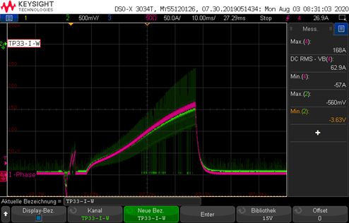
Spikes start at ~80A phase current.

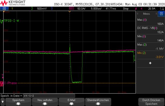
Green is the voltage on SOB,

Red is the current measured with clamp meter.

The DIS_SEN =1b, so the fault is ignored. Is there another protection of the SOA output? Or can you explain what happen in these 5µs?

Rgds Martin

  • Martin,

    Is it possible for you to try a slightly smaller sense resistor?

    Regards,

    -Adam

  • Hi Adam,

    As I mentioned I'm using the rds_on of the low side mosfets for current measurement (2 parallel => rds_on 0.5mR) and I can't change to a sense resistor, because of the PCB space.

    Do you have an explanation for these "spikes", is this a known issue with the rds_on measurement?

    Rgds Martin

  • Hi,

    Are there any updates on this issue?

    Rgds Martin

  • Martin,

    It's hard to say exactly what is causing the spikes but I can tell you that using the FET RDSON for current sensing is not usually recommended. The RDSON from one FET to the next can change quite a bit and the RDSON also varies with temperature.

    Have you checked if you are violating the input max or min for the CSA input?

    Regards,

    -Adam

  • Hi Adam,

    The problems with the RDSON are known and compensated in via software. I didn't find any information, that RDSON measurement isn't recommended with the DRV8323 Driver.

    I checked the CSA input voltages and they are within the spec values.

    Rgds Martin 

  • Martin,

    Did this issue get resolved? Sorry for the delay here.

    Regards,

    -Adam

  • Hi Adam,

    For me it's no really resolved. I still have no answer to the questions:

     "... Is there another protection of the SOA output? Or can you explain what happen in these 5µs?"

     Rgds Martin

  • Martin,

    Have you checked the status of the VREF/VM supplies at the time of the 5us dip? Are you using the SPI or hardware version of the device?

    Regards,

    -Adam

  • Hi Adam,

    I'm using the SPI device. The VREF/VM are ok, the phase current is still flowing during the dip.

    By the way: on the revision history of the index *c* data sheet is no information, that the mechanical data has changed.

    Rgds Martin

  • Martin,

    Are you reading or writing any SPI signals when the dip is seen?

    What about the CAL pin during the dip?

    Can you share your schematic?

    Regards,

    -Adam

  • Hi Adam,

    No, we don't read or write on the SPI at this moment. Also, the CAL pin is "low" all the time.

    When I reduce the IDRIVEP_HS and IDRIVEP_LS currents, the dips disappear. (Old: 820 mA ==> New: 440 mA)

    It seems to me, that there are spikes on the Mosfet switching which, causing the dips. I can’t measure spikes which are out of the specs. So what protect the internal OP for 5µs? Could you check with your silicon specialists?

    Rgds Martin

  • Martin,

    Sorry for the delay here.

    I haven't confirmed what exactly is happening but it sounds to me that you have the IDRIVE configured way too high for your FETs which may be causing some trouble with the CSA.

    What is the Qgd of your FETs and can you show us a schematic snipped of the DRV and FETs?

    Regards,

    -Adam

  • Hi Adam,

    What I didn’t mentioned yet, is that this behavior is only on one phase. The others work fine, no matter which driver current is configured.

    All phases have the same HW-config. The Qgd of one Mosfet is 44nC and we have two parallel because of the high current in our system.

    Rgds Martin

  • Martin,

    Do you observe this on a second board? I'm wondering if you have one DRV  or FET that is bad and causing this issue.

    Regards,

    -Adam

  • Hi Adam,


    Yes, I got this issue on every board (5 pcs) I’ve tested. Unfortunately, no particular case.


    Rgds Martin

  • Hi Martin,

    I took a quick look over all the communication so far and had a few questions that can hopefully lead us to what is causing this glitch. As shown in the datasheet block diagrams, the SOA/B/C outputs do not have protection circuits between them and their phase's CSA output . My first guesses would be to take a look at how VREF, DVDD, and VM behave during the glitch, in case one of the supplies drop out.

    Reviewing the posted schematic, I could not see if there are net ties somewhere for the SPx pins to measure across Rds(on). Would it be possible to take a closer look at where SPx is connected?

    Additionally, based on the fact that this occurs on multiple boards, at higher IDRIVE strength, and only on one phase, I am thinking that this issue might involve coupling. Would you be willing to share layout near the CSA outputs for the phase with the glitch? If you cannot post it here, alternatively you can add me as a friend on E2E and message me directly. If there are switching signals that may be present on the board near the CSA output, scope captures of their behavior during the glitch would also be helpful. Thanks for your time!

    Best regards,

    Omar

  • Hi Omar,


    I measured no voltage drops on the supply pins you mentioned, especially no drops with 5µs, but I’ll recheck. And for me it’s still not clear, why the output signal goes down to 3V (equals 0A) and not to 3.3V or to 0V?!

    The SPx Pins aren’t connected to any net. They’re open like in the datasheet and shorted internally to SNx (I hope). Do I have to short them also outside the driver?

    To the layout questions, there are the power mosfets at the TOP layer over the CSA outputs. But all 3 outputs are parallel, so in my opinion, the behaviour should be the same.

    Rgds Martin

  • Hi Martin,

    The setup you have looks correct, I am fairly certain this issue is going to be on the input side of the CSA though. If you take a look at figure 39 in the datasheet, you can see that the amplifier is not rail to rail. The 0A reading is 0.3V below VREF, which means the 3V readings in unidirectional mode are pointing to a couple possibilities. Either SNx is spiking above SHx, or SHx is spiking negative. I think the latter is more likely, since lowering IDRIVE would decrease the slew rate of SHx. At higher slew rates, parasitic inductance could contribute to this issue.

    To get some clarity on this, we would need to look at a SHx-SNx differential scope measurement. If that is not possible, SHx to GND and SNx to GND individually would be fine. If I could see a capture of GLx and SOx together that would also help me see where the glitches happen with respect to switching of the FET.

    Thanks,
    Omar

  • Hi Omar,

    I measured the Phase A which have the problem.

    Ch1 (yellow): SH_A vs. SNA (measured with a differential probe)
    Ch2 (green): GLA
    Ch3 (blue): SOA
    Ch4 (red): Phase A current, measured with current probe

    As you can see the problem starts at ca. 90A, the lowside is active all the time. The spikes are only in the SOA signal, not in the current which is flowing in the phase.

    Rgds Martin

  • Hi Martin,

    Nothing in that screenshot except for the SOA output appears abnormal so the next place I would take a look at is the layout.

    Regarding IDRIVE, you mentioned the 440mA setting eliminated the problem, correct? Was that lower IDRIVE suitable for your system?

    Thanks,
    Omar

  • Hi Omar,

    The layout is probable the reason, but it still is no explanation for the 5µs spike. This could only come from the driver and I can’t find any hint in the datasheet.

    440mA eliminates the problem, but I would feel better with a little higher driver current and with the knowledge what is happening inside the driver at this "special" state.

    Rgds Martin

  • Hi Martin,

    I checked on the specifications for this part earlier today and there aren't any special states for the built in CSA. However, if we want to try narrowing down where some coupling might be coming from, a scope capture of SOA, SHA, SHB, and SHC on the same screen may give us a hint. It appears that there are might be two issues going on here, one being the 5us spike, and the other looks like coupling to another switching signal   shown alone in the first of the 3 glitches on your last screenshot. I also just wanted to confirm for all the captures of the CSA output, are these measured with respect to GND?

    Thanks,
    Omar

  • Hi Omar,

    Attached the measurements with SOA (blue), SHA (green), SHB (red) and SHC (yellow).
    All measured against GND, also the last measurements with the CSA output were measured against GND.

    Rgds Martin

  • Hi Martin,

    Can you clarify why the SHB and SHC waveforms are different voltages during their on time? If the layout is allowing coupling, then a strong pullup or pulldown of the phases could cause an issue. I think a good next step in this debug is to check the layout. Can you share the layout privately so we may look into this further?

    Best regards,
    Omar

  • Hi Omar,

    Our Motor is in delta configuration. SHA is low, SHC is in complementary mode and SHB is floating. You can see the half battery voltage in this phase.

    I can’t share the layout, because I don’t know if our companies have a valid NDA.

    Rgds Martin

  • Hi Martin,

    Understood, I reached out internally to check on the status of our NDA.

    Best regards,
    Omar

  • Hi Martin,

    After giving this some thought, we should rule out glitching seen on the inputs causing GLA to start to turn off and re-enabling tDRIVE. The best way to test if this might be the source of the issue is by modifying the setting for tDRIVE and checking to see if the width of the 3V pulse changes with it.

    If nothing is seen here, the next step would probably be to look at all three CSA output signals SOA/B/C while the issue is occurring. Also, we do not have a currently active NDA but if it is necessary to help answer your question please let me know and I can start the process of establishing one. Thanks for your patience.

    Best regards,
    Omar

  • Hi Omar,

     I checked the electronics with different tDRIVE settings, first the tDRIVE = 4000ns:


    Next the tDRIVE = 1000ns:


    No difference in the glitch length. On both pictures are all three CSA outputs measured, for me nothing strange.

    Ch1 (yellow): SOB
    Ch2 (green): Phase A current, measured with current probe
    Ch3 (blue): SOA
    Ch4 (red): SOC

     Rgds Martin

  • Hello Martin,

    Just wanted to let you know that there will be some delay in the response as the holiday in the US this week has let to many people taking the week off.

    We'll be sure to respond before 12/4/20.

    Thank you for your patience,

    -Cole

  • Hi Martin,

    I think I have been overlooking an important detail about the SOx scope captures, could you describe further how your scope is connected from TP33 to GND? The reason I ask is because the outputs of SOx should not be negative. Are these SOx-GND or GND-SOx measurements we have been looking at? Also, are there multiple grounds on your board? I was assuming AGND and PGND were tied together at GND in the schematic excerpt you shared.

    Thanks again for your patience,

    Omar

  • Hi Omar,

    The probe is connected to TP33 and the GND clip to the GND-star point. The outputs are not negative, I’ve inverted the signals on the oscilloscope (you can see it at the line over the channel in top line) for a better view of the signals. We’re looking at TP33 to GND measurements, they’re all +3V if there is 0A flowing.

    I only have one GND but routed separate as a DGND and PGND connected at battery input.

    Rgds Martin

  • Hi Martin,

    As an experiment could you short all of the grounds near the DRV8323? It seems like the battery input has a common ground connection while the board itself uses multiple grounds, especially near the device. As a temporary work-around I'd like to see if combining the grounds as close to the DRV8323 as possible would help the issue.

    Best regards,

    Omar

  • Hi Omar,
    I combined all GNDs near the driver, but it makes all worse. Already at lower currents. Here is a picture of phase U:

    Also, the good phase V gets worse:


    Rgds Martin

  • Hi Martin,

    Do you have access to any software tools that would allow for analyzing board parasitics given the layout? It is a bit of a long shot, but if this is an option it may be worth checking out. 

    Best regards,
    Omar

  • Hi Omar,


    Sorry, I don’t have such a tool for analyzing the parasitics on the layout. Do you know a good one, I think the basics should do it in my case?


    Rgds Martin

  • Hi Martin,

    In the past I have seen a few customers using Ansys simulation tools, but I would say this is a far from basic software solution. If it is an option, perhaps we could set up a meeting to look over the layout & schematic via screen share. Please let me know if that is a possibility.

    Best regards,

    Omar