This thread has been locked.

If you have a related question, please click the "Ask a related question" button in the top right corner. The newly created question will be automatically linked to this question.

DRV8312: Mode Pin & PWM pin & GND_A、GND_B、GND_C with Shunt

Part Number: DRV8312

Hi Team,

Need your help Explanation below application issue, thanks

1. 2 mode detailed explanation of behavior patterns

image.png

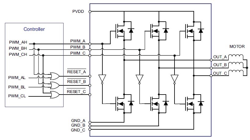
2.What is the application of the PWM pin on the DSP side? The OR gate is necessary? The DRV8312  built-in NOT Gate interlock. When the motor is about to decelerate, How to control the three lower side mosfet to open?

image.png

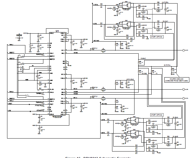
3. Base on referenece circuit, what is the current measured by the receiving shunt resistor at GND_A, GND_B, GND_C pin? Must be contact? measuring the motor phase current, we are should receive the frontend or backend of L2~L4

image.png

  • Kevin,

    Your images did not post, could you please repost them?

    Regards,

    -Adam

  • Hi Team,

    Need your help Explanation below application issue, thanks

    1. 2 mode detailed explanation of behavior patterns

    2.What is the application of the PWM pin on the DSP side? The OR gate is necessary? The DRV8312  built-in NOT Gate interlock. When the motor is about to decelerate, How to control the three lower side mosfet to open?

    3. Base on referenece circuit, what is the current measured by the receiving shunt resistor at GND_A, GND_B, GND_C pin? Must be contact? measuring the motor phase current, we are should receive the frontend or backend of L2~L4
  • Kevin,


      1. Cycle-by-Cycle means that the driver will attempt to reduce the output current by turning off the outputs to allow the current to reduce, at the next PWM cycle the output will enable again and check if the overcurrent still exists. If it was a transient condition that has reduced then the output can continue to work.
      2. Latched mode does not try to reduce the output current, it simply shuts down the driver once an overcurrent has been detected and the output stays off until the driver is manually reset/restarted.
    1. The bridge will be high impedance when RESET is low. To drive the output LOW, RESET must be high and PWM_x must be low. To drive the output High, RESET must be HIGH and PWM_x must be high. The reason for the OR gate is that we want RESET to be high with either the PWM_x is driven high or when the we need the low sides on in which case only RESET needs to be high. The same can be done with MCU logic.
    2. The shunt resistor should measure the current through the bridge as the current flows into GND.

    Regards,

    -Adam