This thread has been locked.

If you have a related question, please click the "Ask a related question" button in the top right corner. The newly created question will be automatically linked to this question.

DRV2700: How to reduce the Boost output ripple

Part Number: DRV2700

Hi Team,

  My customer now is evaluating DRV2700 which worked in BOOST mode,  and they found that the output voltage with higher ripple in low voltage, and increase the Cboost capacitor value, the ripple become bigger.There are capacitors parallelized in Rfb1 and Rfb2, the ripple become worse while removed the parallelized capacitor.

 Could you kindly help to give comments on how to reduce the ripple?

 Below is the schematic, and please noticed that the comments may not correct for the schematic, but the parameters on the schematic are correct.

20200629 - Schematic.pdf

Best Regards

Benjamin

  • Hi Team,

      A little clarification,  the ripple is from OUT+ - OUT-; 

      The DRV2700 worked at boost + Amplifier mode and OUT+ /OUT- differential voltage with higher ripple while with lower output voltage and low ripple with higher output voltage; while increase the C(HV) capacitor, the ripple became higher. and if without the Cfb1/fb2(C93/C47 in schematic), the ripple would become worse.

       Could you kindly give comments on below 2 items:

    1. How to remove the OUT+/OUT- ripple while the DRV2700 worked as BOOST + Amplifier mode;

    2. Which items would involve the ripple?


      DRV2700 Output Ripple Issue.docx

    Best Regards

    Benjamin

  • Hey Benjamin,

    Thank you for reaching out, I will take a look at your schematics and try to respond promptly.

    Best, 

    Carson Allen

  • Hi Carson,

     The key concerns is that while using as Boost + Amplifier mode,  the OUT+/OUT- with lots difference noise,  but if only worked with BOOST mode and used external amplifier, there is no noise at external amplifier difference output. 

     Could you kindly give comments?

    Best Regards

    Benjamin

  • Hey Benjamin

    The ripple depends on the capacitive values at the boost and the input of your waveform and the load you are using, so what is the situation with the input and output?

    This ripple like you said does not output if you have something connected to OUT+ and OUT-  because each output cancels the other one's ripple out, so if that what matters to you than the ripple is fine.

    But to make the ripple smaller, have you tried taking away those two capacitors at the boost and just trying to increase C(HV) by itself

    Best,

    Carson

  • Hi Carson,

      The issue is for the OUT+/OUT- differential ripple, which is abnormal and couldn't be used with internal amplifier if without the capacitor parallelized with Rfb1/Rfb2, and get little bit correction if with the capacitor parallelized the Rfb1/Rfb2.   Enlarger the Chv couldn't fix this issue.

      Other thing is that if add capacitor to OUT+/OUT- which would with a little improvement.

    Best Regards

    Benjamin

  • Hi, Benjamin,

    Due to the internal boost characteristics, the output will show this kind of ripple. The only way to remove the ripple is by adding capacitors at the device outputs. This will decrease the output bandwidth, but it will help to reduce the ripple. In addition, make sure that the VDD is fully stable. Adding capacitors are the VDD pin will also help to reduce the ripple.

    The ripple won't be fully removed, but the differential difference on the load will be used to remove the remaining ripple.

    Best regards,
    Luis Fernando Rodríguez S.

  • Hi Luis,

       As the boost topology, the BOOST output would with the ripple is reasonable,  but the question is the difference differential OUT+ -OUT- still with ripple, which doesn't make sense except there is differential noise. 

      Could you kindly double review the schematic and give solutions for removing differential output noise?\\

    Best Regards

    Benjamin

  • Hi Luis,

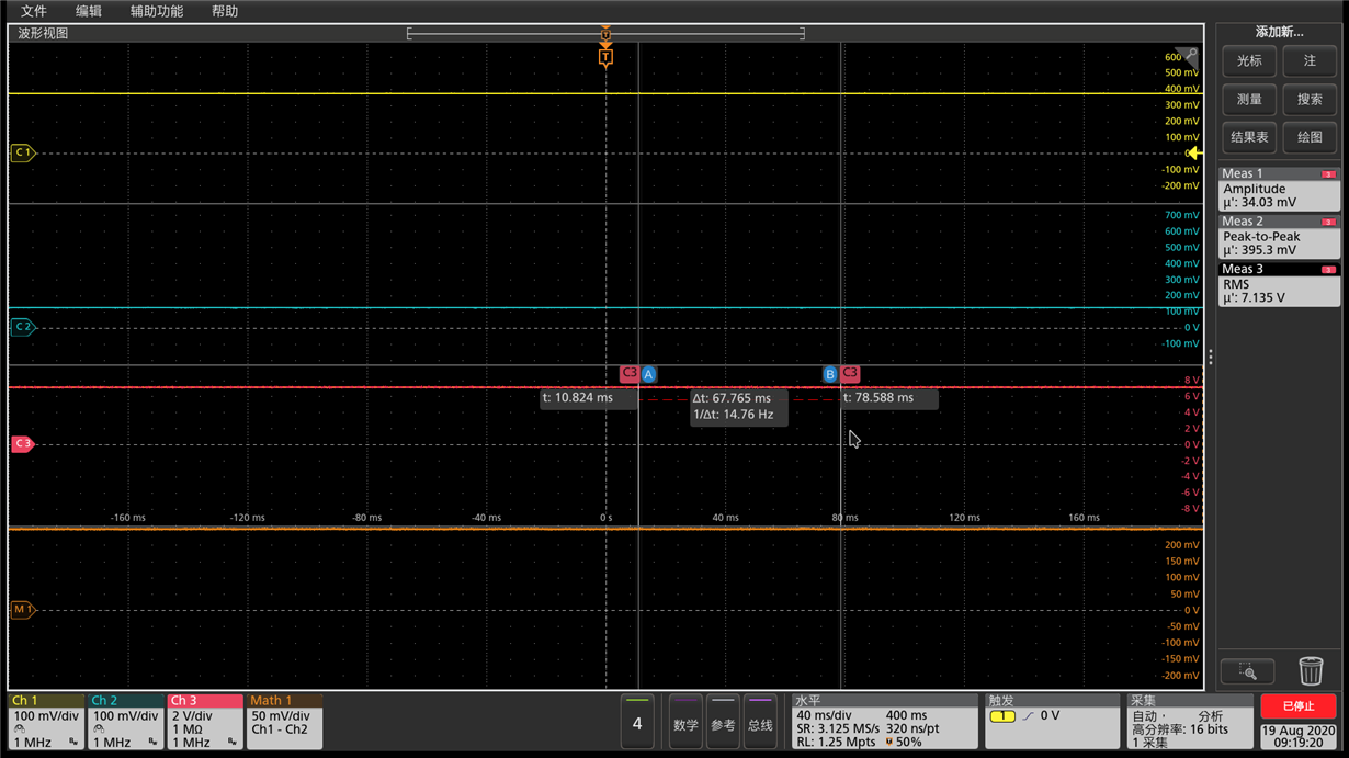
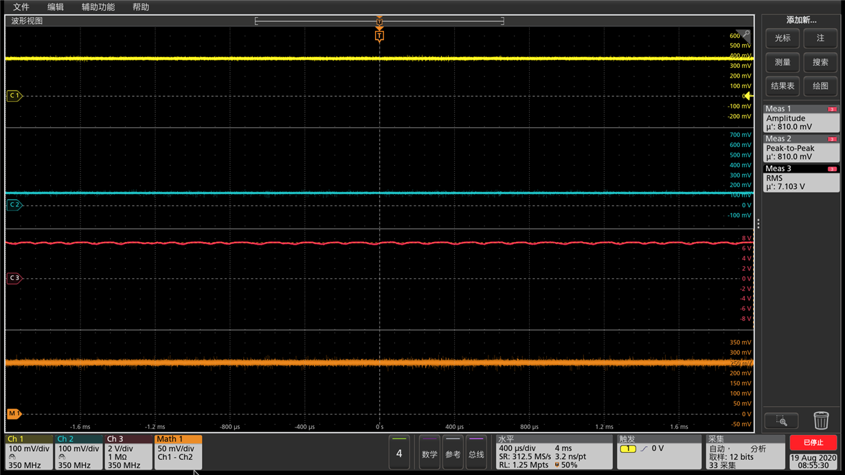
      The differential noise from OUT+ - OUT- is smaller while the PVDD connected to external power source compare to connect to BST pin. 

        -- While PVDD connected to external power source:  The amplitude of (OUT+ - OUT-) is 34.03mv, and Peak-Peak is 395.3mV;

        --While PVDD connected to BST Pin: The amplitude of (OUT+ - OUT-) is 810.0mV, and Peak-Peak is 810.0 mV;

      It seems the BOOST output has affected the OUT+/OUT-,  could you kindly help give comments on how to fix this issue and potential root cause?

      Expect for your kindly reply, thanks.

    Test Waveforms:

      The figure shown the test waveform which connected to external PVDD. 

       C1:  IN+;   C2:  IN-;  Math 1: IN+ - IN-;   C3: OUT+ - OUT-


      The figure 2 shown the test waveform while PVDD connected to BST PIN;

     C1:  IN+;   C2:  IN-;  Math 1: IN+ - IN-;   C3: OUT+ - OUT-

    Best Regards

    Benjamin

  • Hi, Benjamin,

    I just noticed that the DRV2700 doesn't have AC coupling capacitors at the analog inputs in the schematic that you shared. The analog input level is directly related to the differential outputs. Does the customer application require to avoid the use of AC-coupling capacitors?

    Best regards,
    Luis Fernando Rodríguez S.  

  • Hi, Benjamin,

    Excuse me, do you have an update on this?

    Best regards,
    Luis Fernando Rodríguez S.

  • Hi, Benjamin,

    I'm closing this E2E thread due to the inactivity. However, feel free to provide your feedback and observations in case you have them.

    Best regards,
    Luis Fernando Rodríguez S.

  • Hi Luis,

      This issue has been fixed. Thanks for your great support.


    Best Regards

    Benjamin