This thread has been locked.

If you have a related question, please click the "Ask a related question" button in the top right corner. The newly created question will be automatically linked to this question.

DRV8305: About How to use separate power supplies for motor drive power and VCPH, PVDD, VCPH

Part Number: DRV8305

Hi,

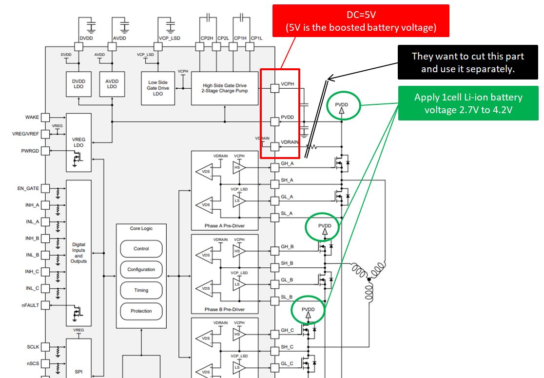
My customer wants to separate the power supply for the motor drive and the power supply for DRV8305.
Is there a problem with the following usage?
(I am checking the background customer want to separate.)


Best regards,
Yusuke

  • Hello Yusuke,

    Thanks posting on the Motor Drive E2E forum!

    Let me get an answer to your question tomorrow (9/9/20 CDT).

    Best,

    -Cole

  • Hi,

    Thank you for your response.

    I understand your situation.
    We look forward to hearing from you tomorrow.

    I provide additional information below regarding this matter.
    Customer's application uses a 1cell Li-ion battery.

    Voltage for driving the DRV8305 itself is driven by 5V obtained by boosting the 2.7V to 4.2V.

    If the power source for driving the motor can be used separately, the power consumed by the booster circuit can be reduced.
    Is there a problem with using DRV8305 like this?

    Best regards,
    Yusuke

  • Hello Yusuke,

    It’s clear that the user wants to use the customer wants to use this part with a motor voltage supply below the recommended operating conditions. While I’m happy that the customer likes the DRV8305, it’s clear that the device wasn’t designed with that low motor voltage in

    The high side gate voltage (as a result of the charge pump), smart gate drive technology (which includes IDRIVE), the protection features (such as VDS monitoring) all depend on the PVDD and VDRAIN values being connected to the motor. If these are bypassed, these will not work at the intended thresholds or cease to function.

    As such, you could try and use this part outside of the recommended voltage range and I can explain all of the losses in performance if you are still interested. But there’s a better device performance, value, and user experience if the customer finds a part that was designed for the customer’s voltage range, even if it’s a competitor.

    Best,

    -Cole

  • Hello Cole,

    Thank you for your kind support.

    >While I’m happy that the customer likes the DRV8305, it’s clear that the device wasn’t designed with that low motor voltage in. 
    >The high side gate voltage (as a result of the charge pump), smart gate drive technology (which includes IDRIVE), the protection features (such as VDS >monitoring) all depend on the PVDD and VDRAIN values >being connected to the motor. If these are bypassed, these will not work at the intended thresholds or >cease to function.

    I reported "above explanation" to the customer.
    If the motor drive voltage and the supply voltage to the DRV8305 are separated,
    Customer would like to make a judgment after knowing the functions that will be lost.

    >As such, you could try and use this part outside of the recommended voltage range and
    >I can explain all of the losses in performance if you are still interested. 

    Thank you for your kind offer.
    Could you tell me the performance information that will be lost for the circuit configuration I sent you?
    And , Could you give me some advice on how to handle the Pin when splitting the power supply in this way?


    Best regards,
    Yusuke

  • Hello Yusuke,

    How to connect:

    Essentially, boost connects to PVDD and VDRAIN, with emphasis on the Boost return paths connected to GND. VCPH should, as you have drawn, connect to PVDD or VDRAIN, which is connected to the boost votlage. All HS FET drains would be connected to the battery.

    We can't leave the SHx nodes floating so they need to be connected to the device to the motor phase (which is where most of the confusion will come from).

    What is lost:

    Here's a list of functions that require extra care:

    • PVDD Undervoltage Fault (PVDD_UVLO) and PVDD Undervoltage Warning (PVDD_UVFL)
    • Minimum boost voltage will determine when the device will trigger this
    • PVDD Overvoltage Warning (PVDD_OVFL)
      • Inductive kick back from motor will not be seen at PVDD as boost will mask it or fail. Maybe not a huge problem given low motor voltage, and possibly low current
    • MOSFET Overcurrent Fault (VDS_OCP) for all low side and high side
      • Depends on VDRAIN and charge pump voltage which are not connected to motor voltage in anyway. So relative scales won't work
      • VDS monitoring and overcurrent protections protect against catastrophic failure. The customer will have to implement their own VDS monitoring
    • Gate Drive Fault (GDF)
      • VGS depends on Gate voltage which depends on charge pump which is, again, not derived from the voltage actually connected to motor
    • The datasheet specs for IDRIVE
      • Internal IDRIVE structure uses PVDD in combination with charge pump and source nodes to generate currents as defined by specs. In general, this will result in higher currents than expected because source node will be less than expected (as a result of a lower motor voltage). Because the mismatch between source and PVDD node, the values will not be calculated correctly
      • This below the recommended applications range, we have not tested and cannot predict what the actual outputs of the current will be. Theory just says it will be "higher"
    • Higher VGS and higher currents
      • FETs of this smaller voltage range usually need less current and VGS to exceed Vth.  This means, we have a very real chance to blow up the FETs if they are not optimized because we will put in more current into the FET.
      • For protection purposes, the customer will be purchasing "bigger" FETs than a competitor would use in the same application. These bigger FETs usually destroy efficiency, higher speeds, layout space, lower thermal efficiency, and other FET dependent performance issues
      • Alternatively, smaller FETs could be tested and, and more likely damaged, which the DRV can't help protect against them
    • Charge pump over and undervoltage (maybe)
      • I will need to double check if there is some instance where the charge pump connections being connected to the boost voltage will cause problems. My prediction is no, but stay tuned for that.

    So, a lot of downsides are protection, but some of it is gate drive architecture. With the protection negated, the customer would have to implement their own versions (at least I would hope so) which adds a lot of needless complexity and cost. But it could be overcome. The gate drive architecture is what is really concerning to me as we have not tested or validated the mismatch between expected source, and gate and drain voltages.  

    Best,

    -Cole