This thread has been locked.

If you have a related question, please click the "Ask a related question" button in the top right corner. The newly created question will be automatically linked to this question.

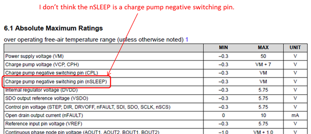
DRV8889-Q1: Absolute Max Rating of nSLEEP Pin

Part Number: DRV8889-Q1

Hello,

In relation to this post, if there is an internal ESD protection diode or internal parasitic diode between nSLEEP pin and VM pin in DRV8889-Q1, I wonder whether a current runs from the nSLEEP pin through the VM pin when a VM voltage drops below 5 V while that 5 V is applied to the nSLEEP pin by an external MCU, for example. I'd like to know if it could happen.

Wang5577 said:
4. I don't see a requirement for a sequencer. But, before nSLEEP pin is pulled high, VM input voltage should be stable. After nSLEEP pin is pulled high at VM>UVLO, please give 0.9ms wake-up time, and then, send signals to DRV8889-Q1. nSLEEP pull-up source cannot use DRV8889-Q1's DVDD.

What's the absolute Max rating of the nSLEEP pin? I wonder if there's something wrong with the Absolute Max Ratings in the data sheet. My question above assumes that the nSLEEP pin's absolute Max voltage is VM.

Best regards,
Shinichi Yokota

  • Hi, Yokota-san,

    That does look like a typographical error. Let us verify that and get back to you early next week.

  • Don,

    I am also checking this issue. nSLEEP pin actually has high voltage ESD structure, so the abs max rating up to VM is correct.

    Further investigation is needed for the current from nSLEEP pin to VM when VM is low. I will reopen this post when I have the answer ASAP.

  • Yokota-san,

    nSLEEP pin voltage range from -0.3V to VM. The next updated datasheet will fix this issue: Delete "Charge pump negative switching pin".

    I got the designer's confirmation:

    "The ESD protection is completely independent for VM & nSLEEP. And there are no parasitic diode paths between VM & nSLEEP.


    There will be no current path from nSLEEP to VM or vice versa, whichever is the power-up sequencing order between VM & nSLEEP."


  • Wang-san,

    Wang5577 said:
    nSLEEP pin voltage range from -0.3V to VM. The next updated datasheet will fix this issue: Delete "Charge pump negative switching pin".

    Then, how should I understand the data sheet specs "Charge pump negative switching pin (nSLEEP): -0.3 V to VM"? According to the 6.3 Recommended Operating Conditions section, VVM can go down to 4.5 V while VI is at 5.5 V, where I assume the VI is nSLEEP pin voltage. If I read the absolute Max ratings strictly, this condition violates it. But, if there is no parasitic current path between VM pin and nSLEEP pin as you confirmed, I guess the condition is acceptable.

    Could you help make this point clear?

    Best regards,
    Shinichi Yokota

  • Yokota-san,

    There are no parasitic diode paths between VM & nSLEEP.  I would think it is OK to have nSLEEP at 5.5V and VM at 4.5V. VM and nSLEEP pin are independent.

  • Wang-san,

    Thanks for your quick feedback. If the "VM" of the absolute Max voltage of the nSLEEP pin is because of its high-voltage ESD structure, I guess the data sheet description might give users a wrong interpretation as I did. If a nSLEEP pin voltage can be higher than a VM pin voltage in a low VVM range, I'd suggest it must be defined differently.

    Best regards,
    Shinichi Yokota

  • Yokota-san,

    Thank you for your feedback. I will pass it to our system engineer to see how to clarify it in next datasheet update.