


Hi Team,
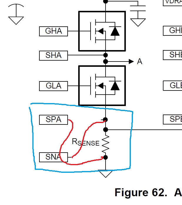
The following figure is the schematic diagram of the current sampling of DRV8323 in the data sheet. Pin SPA is connected to the high side of the sampling Rsense resistor. Pin SNA is connected to the low side of the sampling resistor Rsense.
The customer wants to know if it can be done: SPA is connected to the GND of the sampling resistor, and SNA is connected to the high side of the sampling resistor?
Thanks,
Annie

