


Hi Team,

The picture above is ISEN_A directly from the oscilloscope. If PWM is not given, the bias voltage should be sampled at this time, but the noise is very large at this time. Customer would like to know how to resolve this issue?
Thanks,
Annie
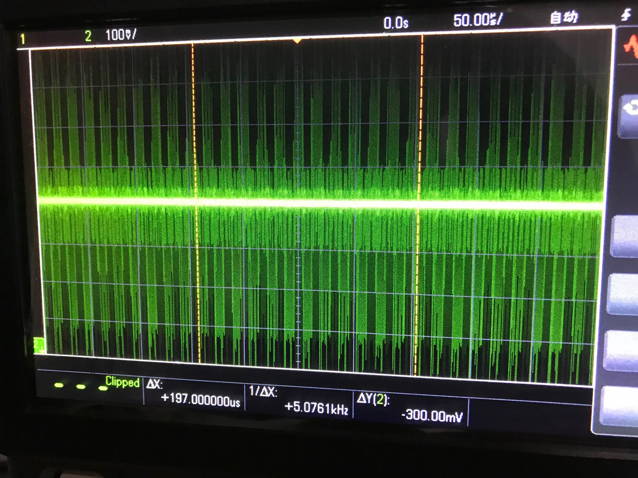
Hi Team,
The picture above is ISEN_A directly from the oscilloscope. If PWM is not given, the bias voltage should be sampled at this time, but the noise is very large at this time. Customer would like to know how to resolve this issue?
Thanks,
Annie
