This thread has been locked.

If you have a related question, please click the "Ask a related question" button in the top right corner. The newly created question will be automatically linked to this question.

DRV8301: GH_A output voltage incorrect

Part Number: DRV8301

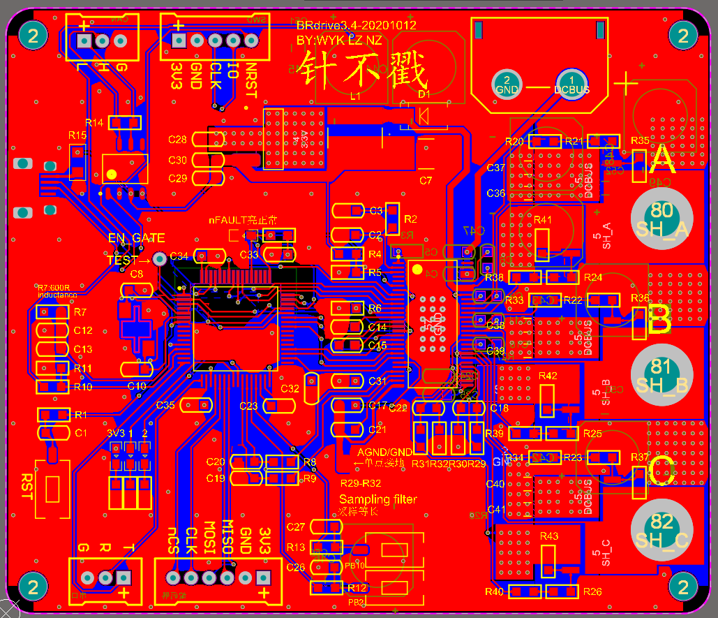
We used DRV8301 to design a motor driver. Up to now, we have made some PCB. But recently the same problem occurred in three different PCB: GH_A output wrong waveform while GH_B and GH_C output the correct waveform.


Here is our schematic: (V3.4)


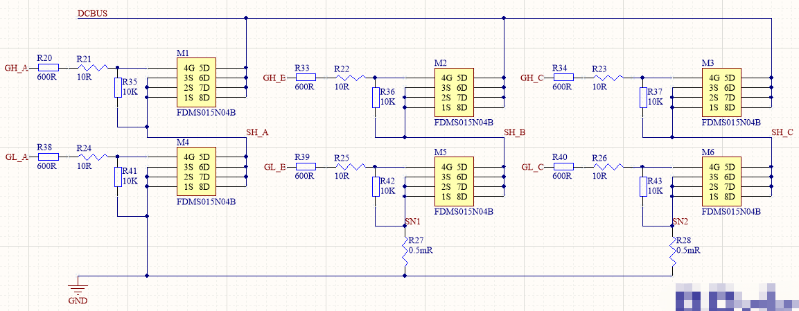
Here is the detail. In all the test bellow, the input voltage of AH/BH/CH was 3V3, while the input voltage of AL/BL/CL was 0V. During all these tests, the nFault were always output high voltage ( No fault were reported.).

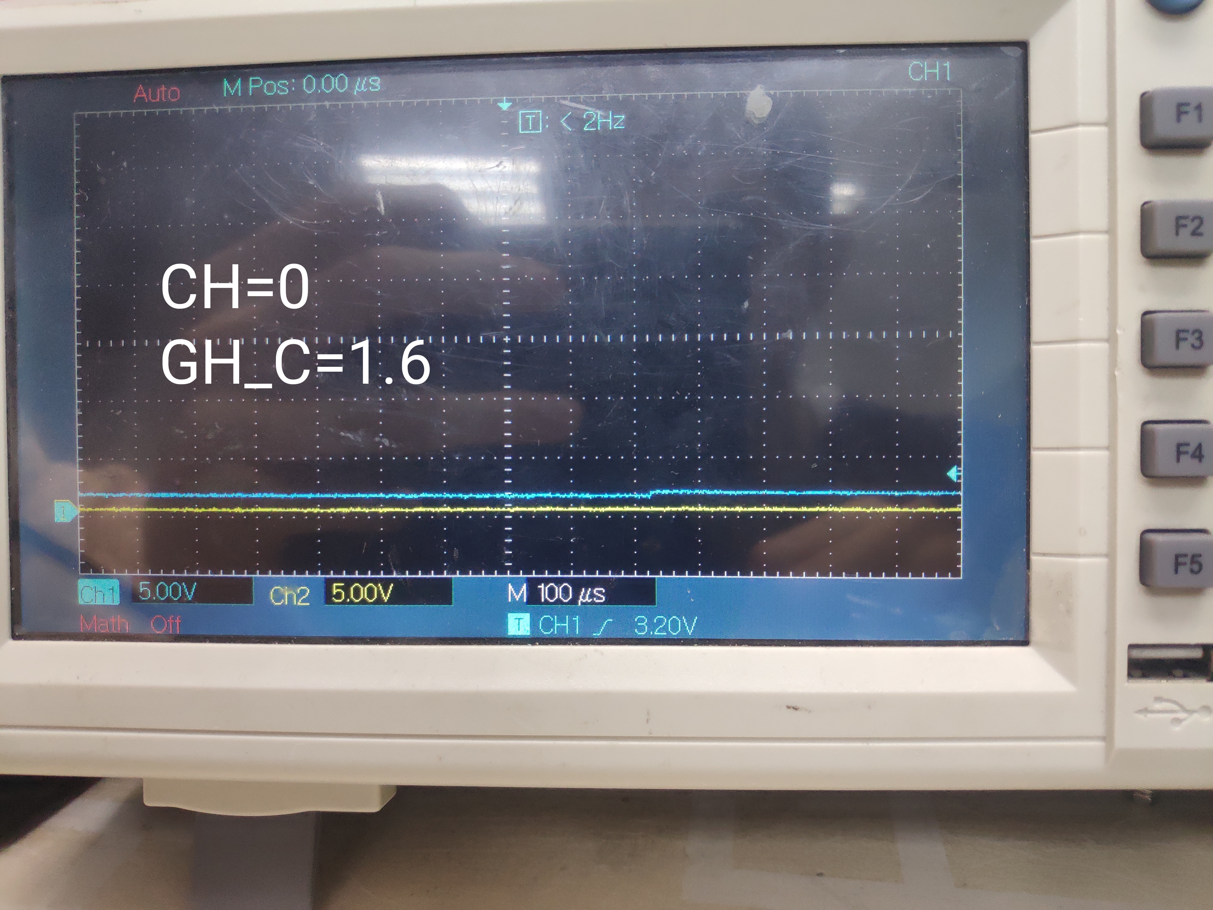
  1. 1.We met this problem for the first time when we were testing one of our Driver version 3.2 PCB. (The other V3.2PCB worked correctly or occurred other problem.) The output voltage of GH_A was around 10V(We didn’t record this waveform. The GH_B and GH_C worked correctly and they were around 30V.). We removed the high-side MOSFET, half-bridge A. But GH_A is still 10V. We welded a new DRV8301 on, but the output voltage of GH_A was still around 10V. We removed the low-side MOSFET, half-bridge A. GH_A became around 1.6V(The waveform looked like the forth V3.4 PCB GH_A figure below.).
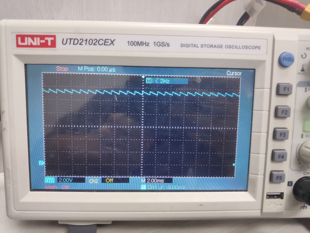
  2. We made a similar PCB version called V3.4. The first PCB of V3.4 worked correctly and it could drive a motor successfully. But we met the “GH_A” problem both in the second V3.4 PCB and the forth one. In the second V3.4 PCB, the GH_A/ GH_B/ GH_C were all 1.6V days ago. Today when AH/BH/CH was 3V3 and AL/BL/CL was 0V, GH_A/ GH_B/ GH_C were all 30V. But when AH/BH/CH and AL/BL/CL input PWM(figure 1), the waveform of GH_A looked like figure 2-5 (The waveform was not stable sometimes.). The waveform ofGH_B/ GH_C were similar as GH_A.


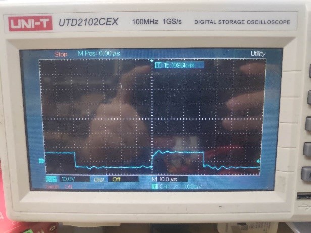
figure 1: input PWM of AH

figure 2: output of GH_A

figure 3: output of GH_A

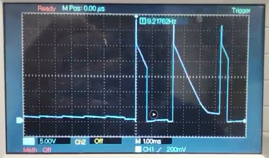
figure 4: output of GH_A

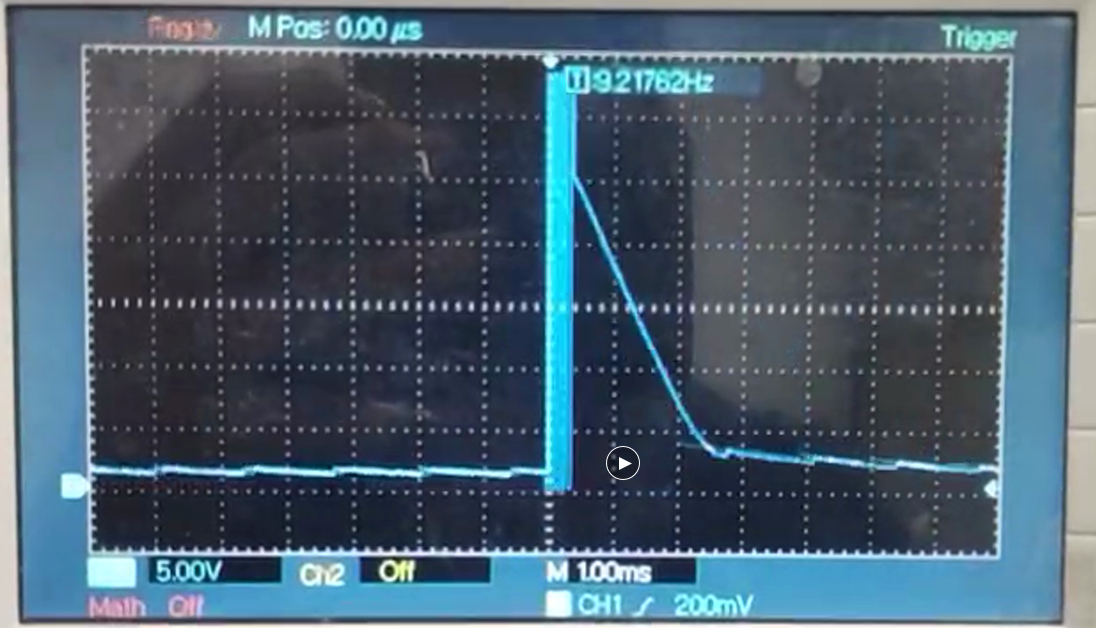
figure 5: output of GH_A


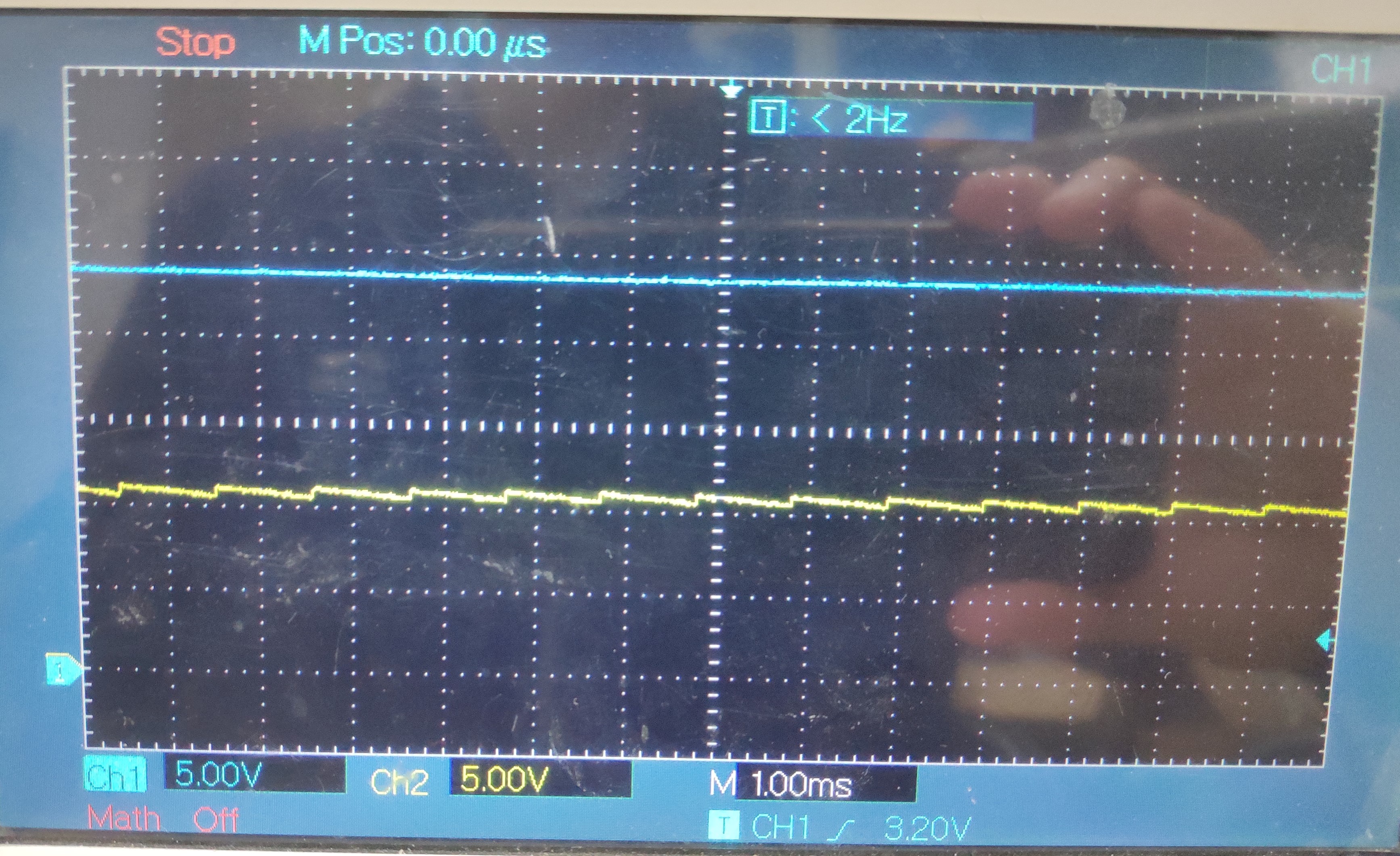
3.In the forth V3.4 PCB, only GH_A was 1.6V. GH_B/ GH_C were 30V. (AH/BH/CH was 3V3, while AL/BL/CL was 0V.) We recorded the waveform of the forth V3.4 PCB. The waveform were recorded in the figure below.


The waveform of the forth V3.4 PCB GVDD:

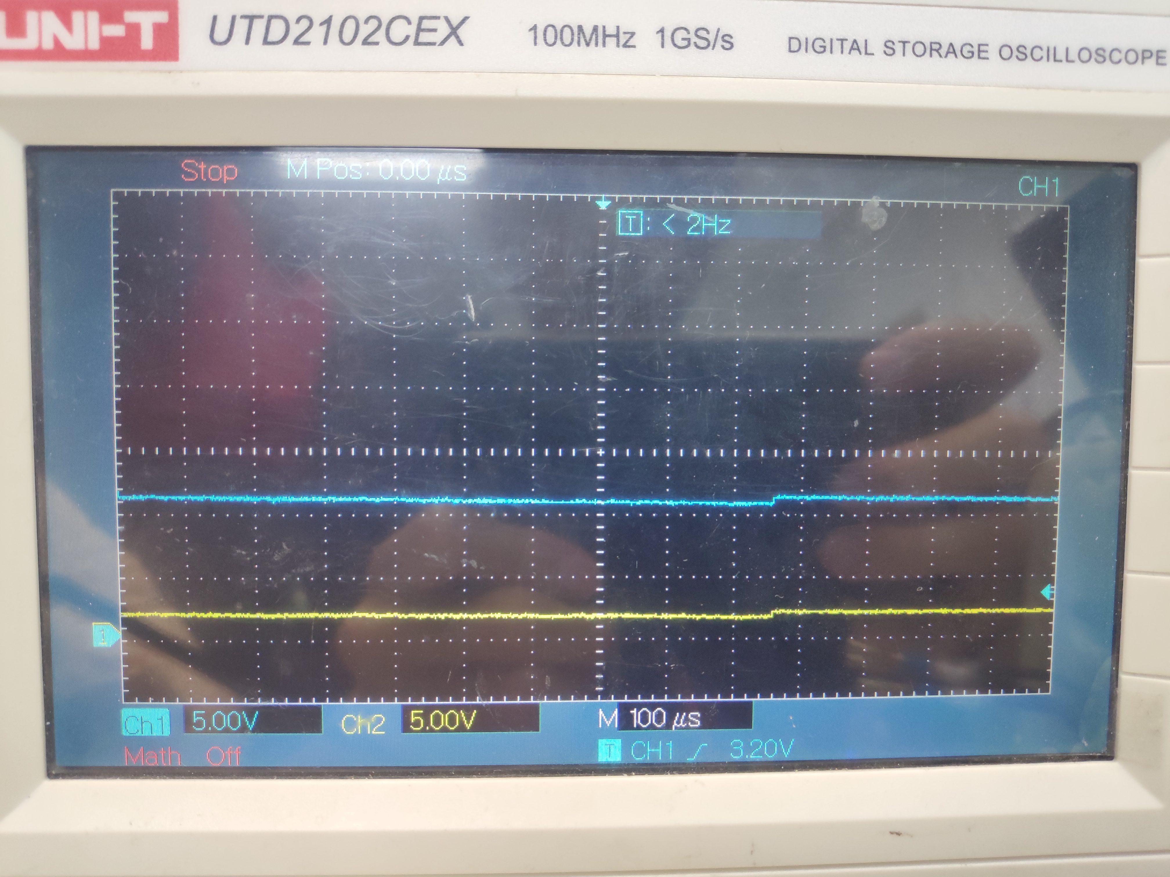
The waveform of the forth V3.4 PCB GH_A

The waveform of the forth V3.4 PCB GH_B:

The waveform of the forth V3.4 PCB GH_C:

  • Hi Leib-Niz,

    For the V3.4 PCB, I would first like to see a scope capture of PVDD1 and GVDD. It is also possible that a layout or assembly issue could be causing this, please refer to this layout best practices guide for suggestions.

    Thanks,
    Omar

  • Hi Omar,

    Thank you for your replying!

    Here is the waveform of the forth V3.4 PCB. The yellow one is GVDD and the blue one is the PVDD1. ( GH_A was 1.6V. GH_B/ GH_C were 30V. AH/BH/CH was 3V3, AL/BL/CL was 0V.) 

    It's maybe  a layout or assembly issue. But the first V3.4 PCB worked well whithout this "GH_A" problem and we haven't find any serious abnormality in its waveforms.

    Regards,

    Leib-Niz

  • Hi Leib-Niz,

    I have a couple questions for you that may help me figure out what is going on here.

    • Have you toggled the inputs for a few cycles to ensure that it is only a select couple boards that have had this issue? If not, I am curious about whether this occurs intermittently but affects all boards.
    • If you give AH=3.3V with BH & CH=0V on a "bad" board, does GH_A turn on normally? I've only seen what appears to be the situation where all 3 phases have their high sides turn on at the same time.
    • Have you looked at BST_A and SH_A? We should take a look at BST_A and SH_A on the same plot for both AH = 3.3V and 0V cases. For comparison it would be good to take a look at BST_B and SH_B.

    Best regards,
    Omar

  • Hi Omar,

    Thank you for your replying!

    We have done some more test. Here is the detail.

    • The forth V3.4 PCB: 

    input : AH/BH/CH 3V3 ; AL/BL/CL 0

    output:  We didn't change the program. So the waveforms are the same as the figures in the first post above.

    Here is some more scope capture.

    figure 3-1 : blue-BST_A ; yellow-SH_A

    figure 3-2 : blue-BST_B ; yellow-SH_B

    For some unknown reasons, we can not upload new program to The forth V3.4 PCB. So we can not change AH/BH/CH or else. We have to use The second V3.4 PCB to continue our tests.

    • The second V3.4 PCB: 

    1. 

    input : AH/BH/CH 3V3 ; AL/BL/CL 0

    output: GH_A/B/C around 1.6V ;  GL_A/B/C 0 . The waveform of BST_A/B/C and SH_A/B/C are the same as figure 3-1.

    2. Change program

    input : AH/BH/CH 0 ; AL/BL/CL 3V3

    output: GH_A/B 0 ; GH_C around 1.6V ;  GL_A/B/C around 12V .  

    figure 3-3 : blue-BST_A/B/C   ; yellow-GL_A/B/C( the same asGVDD)

    figure 3-4 : blue-GH_C  ; yellow-none

    3. Change program 

    input : AH/BH/CH 0 ; AL/BL/CL 0

    output: GH_A/B/C around 1.6V ;  GL_A/B/C 0 .  

    figure 3-5 :  blue-BST_A/B/C ; yellow-GH_A/B/C

    Thanks,

    Leib-Niz

  • Hi Leib-Niz,

    I noticed you have 600 ohm series gate resistors, this is likely too much. A 10 ohm resistor per gate should be sufficient. As an experiment, can you retry your tests after removing all the 600 ohm resistors and replacing them with 0 ohm resistors?

    Also, could you attach some pictures of the PCBs during operation?

    Thanks,
    Omar

  • Hi Omar,

    The 600 ohm are not resistors. They are  bead inductance.

    We only used 10 ohm per gate in V3.2. But the waveform  oscillated(figure 4-1). So we add 600R bead inductance in order to eliminate gate oscillations. And it is proved that the beads are effective in eliminate gete oscillations.

    figure 4-1 : The third V3.2 PCB GL_A

    By the way, in the fifth V3.2 PCB without 600R bead, we also meet the "GH_A" problem (GH_A around 1.6V).

    Here is our V3.4 PCB(four layers):

    figure 4-2:

    figure 4-3:

    figure 4-4:

    figure 4-5:

  • Hi Leib-Niz,

    Regarding the V3.2 gate oscillation:

    • Is scope screenshot 4-1 a GL_A measurement referenced to GND? If not, what is this in reference to?
    • What was your setting for gate current? If it was set to the default, this is actually the maximum gate current. On the V3.4 board that you are able to program, would it be possible to turn the gate current setting in register 0x02 to the minimum and replace the ferrite beads with shorts as mentioned previously?

    For more information about choosing the gate drive current and sizing the gate resistance, please take a look at this FAQ.

    Thanks,
    Omar

  • Hi Omar,

    I am so sorry for I didn't reply for such a long time.

    • Yes, the scope screenshot 4-1 a GL_A measurement referenced to GND.
    • We use the default gate current. We will try different gatecurrent setting later. 

    We have made some more V3.4PCB, and we have tried to fix the PCBs with GH 1.6V problem. 

    1. The second V3.4 PCB used to have GH 1.6V problem. And we changed( reweld ) a drv8301. Then it worked well without any problem.
    2. As we have successfully fix a PCB, we tried to use the same method to fix other PCB( the 3rd and the 5th V3.4PCB) . But we failed to fix any of them. We have rewelded at least three drv8301 to the 3rd V3.4PCB but the GH_A was always 1.6V and GH_B/C was always 30V(correct value). The 5th V3.4PCB made a "splatter" noise at first( We didn't weld MOSFET.). The nfault LED shouted down( nFault LED should be bright when drv8301 works correctly.). We rewelded a drv8301, the noise changed into a sound like buzzer sound. We thought the BUCK circuit in drv8301 maybe not working correctly. The Input current of PCB was about 20mA ( a correct value). But when we pressed and holded the RESET button, the noise weakened and the Input current of PCB became about 0mA. We rewelded a drv8301 again and it didn't make noise any more and the nFault LED was bright. But unfortunately, the GH_A/B/C were all 1.6V.
    3. We welded the 6th V3.4PCB. without MOSFET. The nFault LED was light up. GH_A was 1.6V and GH_B/C was 2.5V. They were all incorrect.

    What puzzled us most is that while the GH is 1.6V, the SH is also 1.6V. We think the SH act as a independent wire. When high-MOS open, the SH will be 24V. When low-MOS open, the SH will be 0V. When high-MOS and low-MOS close, the SH should not be same as GH. We suspected there was a short circuit between GH-SH in drv8301. So we measured the resistance between GH-SH-GL. The GH-SH in A/B/C were all about 1MΩ in 3rdPCB and were all about 4MΩ in 5th and 6th PCB.  The GL-SH in A/B/C were all about 11MΩ in 3rdPCB and were all about 16MΩ in 5th and 6th PCB.  These proved that there were no short circuit in drv8301.

    Are there any possibility that the GH1.6V problem were all caused by drv8301 because drv8301 were broken down?

    Thanks,

    Leib-Niz

  • Hello Leib-Niz,

    For your information, we're getting close to a national holiday in the US so I ask for your patience as response times might be delayed, as people (like Omar) will be taking time off.

    For the gate ringing:

    I just want to reiterate Omar's advice, please make sure you test the lower gate drive current. This should help reduce the gate ringing oscillations. Less current means less energy coupling through parasitic capacitances and weaker electric fields radiated by the gate trace (which could couple into other circuits).

    Adding the ferrite beads in the path add inductance in the path which is not recommended design as inductance will cause ringing and oscillations as the L interact with the C of the FETs and gate traces. Replace with them with low resistances, as Omar suggested, to help with these.

    SH act as a independent wire [from GH]:

    This is mostly true. We know that the voltage on the gate of the MOSFET needs to be higher than the source voltage in order to turn on. This satisfices V_GS > V_th. But we know the MOSFET has to be off if V_G - V_S = 0V, or V_G = V_S. This is why R41 - R43 exist on your board correct? To allow current to flow out of the gate and to the source node until I = 0A between the two nodes (which means V_G and V_S would be at the same voltage).

    In addition, pulling the ENABLE pin to an off state will enable pull down within the GHx pin of the DRV8301 and start to pull current out of the gate and push it to the SHx pin. This is represented by the R_gate_off spec in the datasheet

    Guessing by the M ohm measurements, you probably measured it when the device was enabled but no pulling of the gates high. This would at least mean there isn't a short from gate to GND, but did you compare against a known good board and device to see if they were similar?


    Soldering (or welding) and Debug:

    Based on everything I've read, you still haven't figured out if the problems are caused by the boards or the device, correct? You've replaced devices but have put "bad" devices on "good" boards to see if the problem follows the device or the board? Please, correct me if I'm wrong.

    There is a problem with this, it sounds like the soldering (or welding) is not being done by manufacturer when replacing the DRV. If the re-weld process is not using solder paste, a heat gun, and a board warmer; or a specialized solder reflow machine, then we cannot be sure the welding work is up to the quality of a manufacturer. This means, there's a chance for a good part to fail, regardless of good or bad boards, because the device isn't connected to the board properly. Be sure to factor this into the debug.

    Best,

    -Cole